Plasma processor, wafer jacking device and method thereof

A lifting device and plasma technology, applied in the field of ion treatment, can solve the problems of unstable movement, difficult installation accuracy, slag removal, etc., and achieve the effects of improving installation and work efficiency, ensuring safe separation, and good coaxiality

A lifting device and plasma technology, applied in the field of ion treatment, can solve the problems of unstable movement, difficult installation accuracy, slag removal, etc., and achieve the effects of improving installation and work efficiency, ensuring safe separation, and good coaxiality

CN112447579APending Publication Date: 2021-03-05ADVANCED MICRO FAB EQUIP INC CHINA

Image

  • Plasma processor, wafer jacking device and method thereof
  • Plasma processor, wafer jacking device and method thereof
  • Plasma processor, wafer jacking device and method thereof

Examples


Embodiment Construction

[0033]In order to make the purpose, technical solutions and advantages of the embodiments of the present invention clearer, the technical solutions in the embodiments of the present invention will be clearly and completely described below in conjunction with the drawings in the embodiments of the present invention. Obviously, the described embodiments It is only some embodiments of the present invention, but not all embodiments. Based on the embodiments of the present invention, all other embodiments obtained by persons of ordinary skill in the art without making creative efforts belong to the protection scope of the present invention.

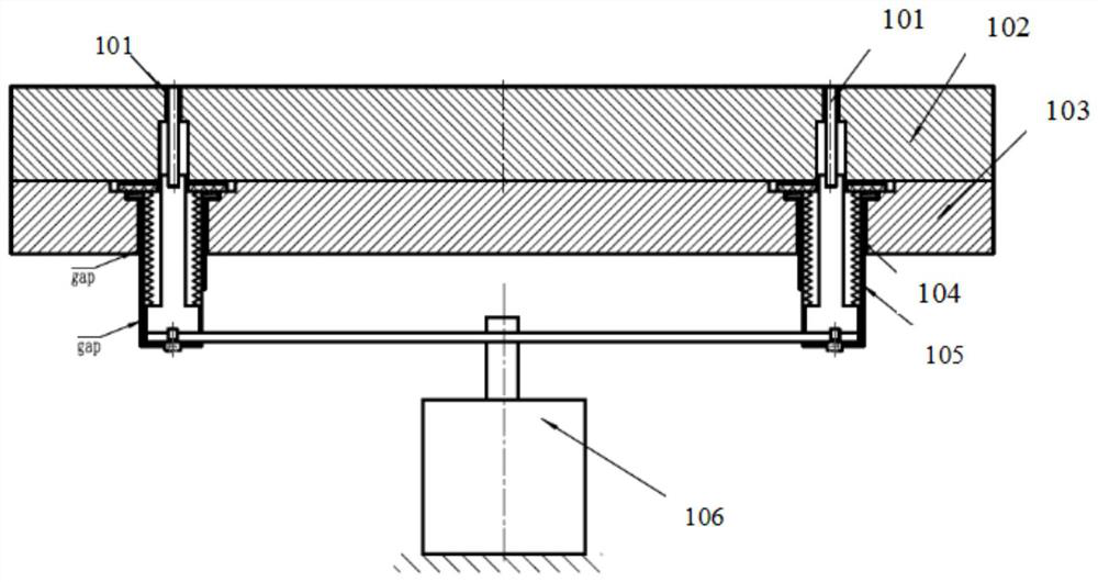
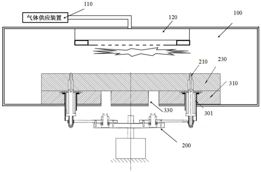
[0034] Such as figure 2 As shown, the plasma processor of the present invention includes a vacuum reaction chamber 100, and the vacuum reaction chamber 100 includes a substantially cylindrical reaction chamber side wall made of a metal material. A gas shower device 120 is arranged above the side wall of the reaction chamber, and the gas show...


PUM


Abstract

The invention discloses a plasma processor, a wafer jacking device and a method thereof. A base is arranged in a reaction cavity, a mounting plate is arranged below the base, the base and the mountingplate are provided with through holes to form a guide channel, and the wafer jacking device comprises an ejector pin assembly at least partially located in the guide channel, wherein the ejector pinassembly comprises an ejector pin and an ejector pin central shaft for driving the ejector pin to lift, and a sealing corrugated pipe is arranged outside the ejector pin central shaft; a driving assembly which is used for driving the ejector pin to ascend and descend in the guide channel; a height adjusting assembly which comprises a height-adjustable support, wherein the height-adjustable supportis connected with the center shaft of the ejector pin and an adjusting screw; wherein a height adjusting hole is formed in the mounting plate in a penetrating mode and used for containing a height adjusting tool and rotating the adjusting screw, height adjustment of the height-adjustable support is achieved, and the height adjusting tool is detachably located in the height adjusting hole. According to the invention, the high levelness of the top ends of the plurality of thimbles can be ensured; the height of the thimble can be directly adjusted above the mounting plate in the reactor, so thatthe working efficiency is improved.

Description

technical field [0001] The invention relates to plasma processing, in particular to a plasma processor, a wafer jacking device and a method thereof. Background technique [0002] In semiconductor wafer processing equipment, when the wafer is transported between the transfer chamber and the vacuum processing chamber, it is necessary to use a lifting device to raise or lower the wafer to realize the wafer leaving the surface of the electrostatic chuck or falling to the surface of the mechanical arm, so as to realize the The electrostatic chuck is detached or leaves a height space for the robotic arm to take the sheet. [0003] In the process of electrostatic adsorption and desorption between the wafer and the electrostatic chuck, there are very high requirements on the parallelism and height of the surface of the wafer and the electrostatic chuck, that is, the height of the lifting device supporting the wafer and the top of the three thimbles. There are very high requirements...

Claims


Application Information

Patent Timeline
05 Mar 2021
Publication
CN112447579A
IPC
H01L21/687; H01J37/32; H01J37/20
CPC
H01J37/32715; H01J37/20; H01L21/68742; H01J2237/334
Inventors
苏宜龙; 蔡楚洋