Method for processing diffused high-sheet-resistance silicon wafer

A treatment method and high square resistance technology, applied in the direction of sustainable manufacturing/processing, electrical components, climate sustainability, etc., can solve the problems of increased production cost, reduced conversion efficiency, high fragmentation rate, etc., and achieve an increase in the rate of A-grade products , the effect of improving the rate of A-grade products and improving the conversion efficiency

Inactive Publication Date: 2021-03-05
HAINAN YINGLI NEW ENERGY
View PDF7 Cites 0 Cited by
  • Summary
  • Abstract
  • Description
  • Claims
  • Application Information

AI Technical Summary

Problems solved by technology

[0005] After the texturing process is the diffusion process. In the process of diffusion production, the process is terminated due to abnormal equipment or flash off of peripheral equipment, resulting in frequent occurrence of unqualified surfaces with high diffusion resistance. Oxide, no direct secondary diffusion
The traditional processing method is to return to the first process of texturing. The direct result of this method is that the silicon wafer becomes thinner and the production cost increases. The chip fragmentation rate is much higher, and the surface chip of the unqualified silicon chip with high square resistance undergoes secondary texturing to produce bright cells, resulting in a decrease in short-circuit current and short-circuit voltage, and a decrease in conversion efficiency, thereby increasing production costs

Method used


Image

  • Method for processing diffused high-sheet-resistance silicon wafer
  • Method for processing diffused high-sheet-resistance silicon wafer
  • Method for processing diffused high-sheet-resistance silicon wafer

Examples


Embodiment Construction

[0033] The following will clearly and completely describe the technical solutions in the embodiments of the present invention with reference to the accompanying drawings in the embodiments of the present invention. Obviously, the described embodiments are only some, not all, embodiments of the present invention. Based on the embodiments of the present invention, all other embodiments obtained by persons of ordinary skill in the art without making creative efforts belong to the protection scope of the present invention.

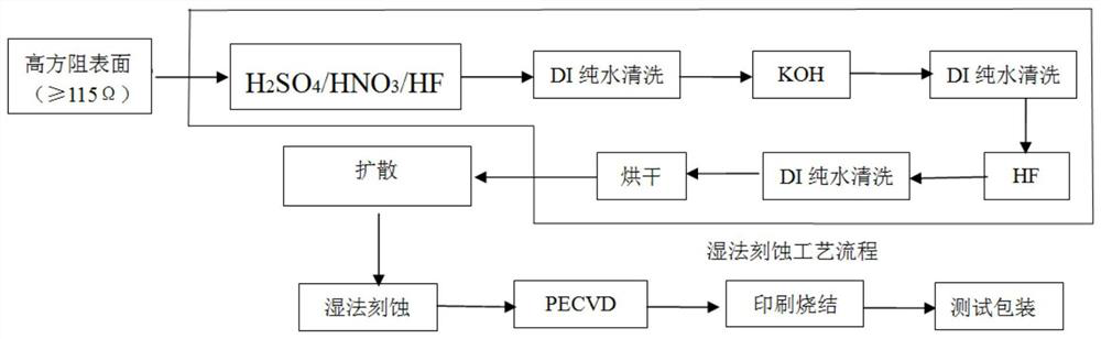
[0034] attached figure 2 It is a flow chart of the treatment of high square resistance battery diffusion sheet in the scheme of the present invention, refer to figure 2 As shown, the present invention claims a method for processing a diffused high-resistivity silicon wafer, comprising the following steps:

[0035] S1: Put the diffused high square resistance silicon wafer into the H 2 SO 4 / HNO 3 / HF mixed solution for secondary etching, the etching depth...


PUM


Abstract

The invention provides a processing method for a diffused high-sheet-resistance silicon wafer, and the method comprises the following steps: S1, enabling the diffused high-sheet-resistance silicon wafer to be placed in a mixed solution of H2SO4/HNO3/HF for secondary etching, and enabling the etching depth to be (1.0-1.2) [mu]m; S2, cleaning the etched silicon wafer with the high sheet resistance by using DI pure water; S3, removing the porous silicon structure on the surface of the high-sheet-resistance silicon wafer by using a KOH solution; S4, performing DI pure water cleaning; S5, removingthe oxide layer on the surface of the high-sheet-resistance silicon wafer by using an HF solution; S6, performing DI pure water cleaning; S7, performing drying in a drying tank; S8, transferring the dried high-sheet-resistance silicon wafer into the diffusion process again for secondary diffusion, wherein the secondary diffusion temperature is 10-30 DEG C lower than the conventional diffusion process temperature; S9, carrying out secondary etching on the high-sheet-resistance silicon wafer after secondary diffusion to improve the back polishing effect, and then transferring to a normal production process.

Description

technical field [0001] The invention relates to the technical field of photovoltaic cell production, in particular to a method for processing a diffused high-resistance silicon wafer. Background technique [0002] As a green and environmentally friendly new energy source, solar cells have attracted worldwide attention. The global photovoltaic industry is developing very rapidly, and the domestic photovoltaic industry continues to grow. [0003] With the continuous development of the industry, customers have higher and higher requirements on the performance and appearance of solar cells, and low-wattage modules and flower modules have been eliminated by the market. Only by continuously reducing production costs can enterprises survive in the market. Improving conversion efficiency is one of the most effective ways to reduce production costs. [0004] The texturing process is the most important step in the battery production process. Its purpose is to use the mixed solution...

Claims


Application Information

Patent Timeline
Patent Type & Authority Applications(China)
IPC IPC(8): H01L31/18
CPCH01L31/1804Y02P70/50
Inventor 曾德栋陈议文
Owner HAINAN YINGLI NEW ENERGY
Why Eureka
Try Eureka