Micro-fluidic chip welding method

A technology of microfluidic chips and welding methods, applied in welding equipment, laser welding equipment, manufacturing tools, etc., can solve the problems of reducing the height of transparent glass media, affecting materials, heating, etc.

A technology of microfluidic chips and welding methods, applied in welding equipment, laser welding equipment, manufacturing tools, etc., can solve the problems of reducing the height of transparent glass media, affecting materials, heating, etc.

CN112454914AInactive Publication Date: 2021-03-09广东华焯激光科技有限公司 +1

Image

  • Micro-fluidic chip welding method
  • Micro-fluidic chip welding method
  • Micro-fluidic chip welding method

Examples


no. 1 example

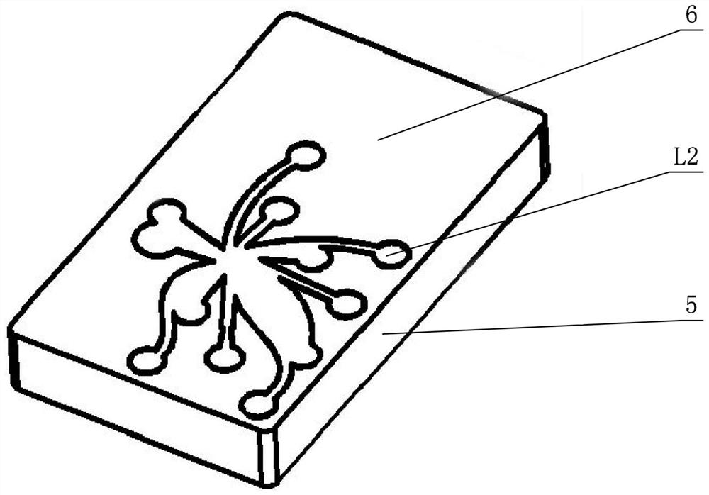
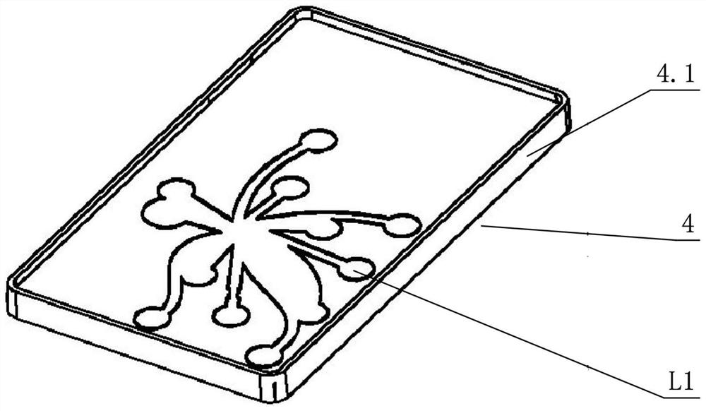
[0035] see Figure 1-Figure 7 , a microfluidic chip welding method, comprising a welding fixture 1, a laser welding head 2, a motion platform 3 for controlling the movement of the laser welding head 2, a microfluidic chip 4 and a light-transmitting plate 5 respectively placed on the welding fixture 1, Its welding method comprises the following steps:

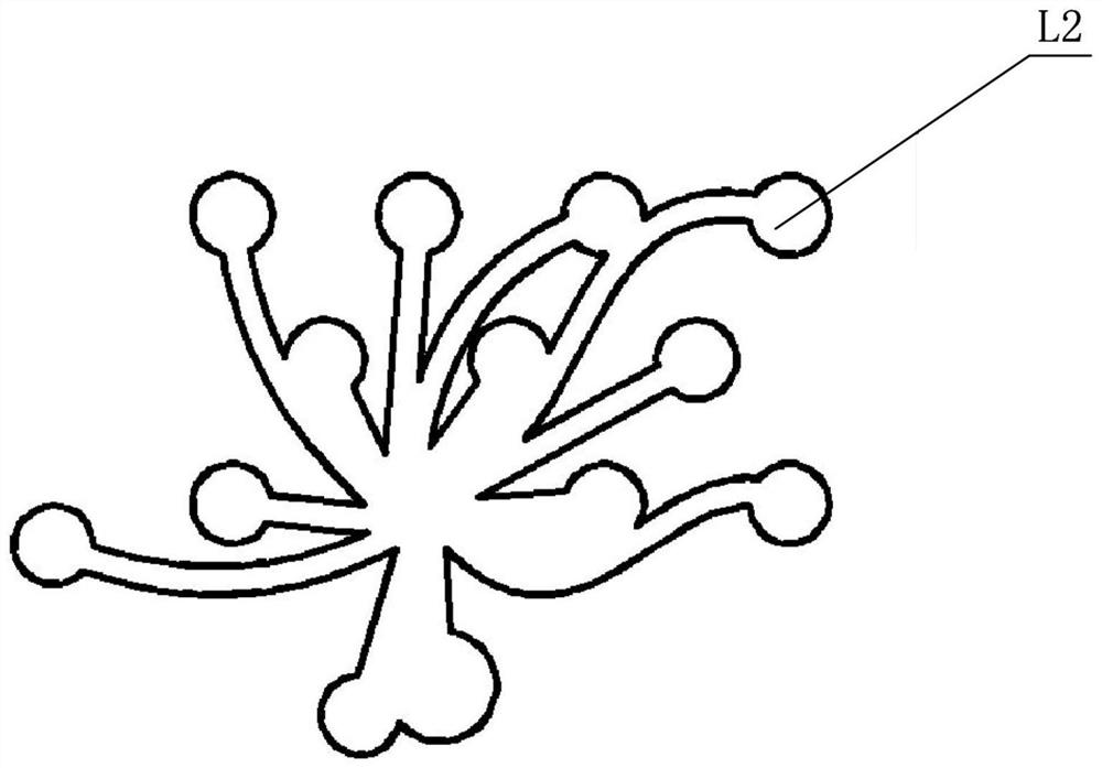
[0036] a. Coat a layer of light-shielding material 6 on the light-shielding material 6, and perform laser marking on the light-shielding plate 5 coated with the light-shielding material 6. During the laser marking, according to the channel path L1 of the microfluidic chip 4, the Part of the light-shielding substance 6 is removed to form a light-transmitting path L2 consistent with the flow path L1 on the light-transmitting plate 5;

[0037] b. The microfluidic chip 4 is covered with a thin film 7, and the microfluidic chip 4 covered with the thin film 7 and the light-transmitting plate 5 are respectively clamped on the welding ...

no. 2 example

[0059] A microfluidic chip welding method is different from the first embodiment in that: laser welding uses a semiconductor laser with a laser wavelength of 900-1000nm to achieve welding of a transparent film and an opaque substrate.

[0060] Other parts not described are the same as those of the first embodiment, and will not be described in detail here.

no. 3 example

[0062] A microfluidic chip welding method is different from the first embodiment in that laser welding uses a semiconductor laser with a laser wavelength of 1700-2000nm to achieve welding of transparent films and transparent substrates without adding light absorbing agents.


PUM

PropertyMeasurementUnit
thicknessaaaaaaaaaa
surface roughnessaaaaaaaaaa

Abstract

The invention discloses a micro-fluidic chip welding method. The micro-fluidic chip comprises a welding fixture, a laser welding head, a moving platform for controlling the laser welding head to move,a micro-fluidic chip and a light-transmitting plate, the micro-fluidic chip and the light-transmitting plate are placed on the welding fixture respectively, and the micro-fluidic chip welding methodcomprises the following steps that the light-transmitting plate is plated with a layer of shading matter, and part of the shading matter is removed through laser marking; and a light-transmitting pathL2 consistent with a flow path L1 is formed on the light-transmitting plate; the micro-fluidic chip and a thin film are pressed by the welding fixture, the light-transmitting plate is irradiated by linear laser, the moving platform drives the laser welding head to move, and laser energy released by the laser welding head is absorbed and converted into heat energy by the micro-fluidic chip throughthe light-transmitting plate, so that a contact area between a micro-fluidic channel of the micro-fluidic chip and the thin film is melted to form a welding seam; and laser welding of the micro-fluidic chip and the film is completed. According to the micro-fluidic chip welding method, micro-fluidic channel welding with the width of 0.1 mm can be achieved; and welding can be completed through one-time scanning by adopting the line light source, and the welding efficiency is greatly improved.

Description

technical field [0001] The invention relates to the technical field of laser welding, in particular to a microfluidic chip welding method. Background technique [0002] Generally, the trajectory of the micro-channel is relatively complex and relatively thin. During welding, on the one hand, it is necessary to control the trajectory of laser welding, and it is difficult to control the finer laser trajectory. For example, if the difference is 0.1mm or 0.2mm , it is more difficult to control; on the other hand, if the weld is very thin (narrow width), the welding position is also very thin. That is to require that the spot be controlled to be very small, and then the control of the spot is small, which will lead to the concentration of laser energy and burn out the product; in addition, for this very narrow weld, the beam emitted by the laser will have a thermal effect, which will cause Affects the material next to the weld, making the product unsightly. [0003] Therefore, t...

Claims


Application Information

Patent Timeline
09 Mar 2021
Publication
CN112454914A
IPC
B29C65/16; B29C65/78; B23K26/362
CPC
B29C65/1635; B29C65/1654; B29C65/7841; B29C66/9261; B23K26/362; B23K2101/007
Inventors
丁斌; 潘奇才