Circuit board welding method, circuit board and electronic equipment

A welding method and technology of electronic equipment, applied in welding equipment, metal processing equipment, printed circuit assembly of electrical components, etc., can solve the problems of increasing investment in welding production inspection, difficulty in finding and cleaning up, abnormal operation of equipment, etc., and achieve saving Equipment inspection and manual inspection links, providing reliability and service life, and reducing production costs

Active Publication Date: 2021-03-12
INSPUR SUZHOU INTELLIGENT TECH CO LTD
View PDF2 Cites 0 Cited by
  • Summary
  • Abstract
  • Description
  • Claims
  • Application Information

AI Technical Summary

Problems solved by technology

For example, servers and computer motherboards are soldered with thousands of electronic components. These components often have strict requirements during the soldering process. For example, in order to prevent the serial / parallel connection between components from being damaged or losing their original functions, solder balls cannot be produced during soldering. ;In addition, solder balls are easy to vibrate randomly during the working process of the server and cause a short circuit on the motherboard. Due to the small size of such solder balls, it is difficult to find and clean them all during the soldering process, which brings greater safety and performance to electronic equipment. Hidden dangers, and even lead to abnormal operation of the entire equipment, so the welding process is particularly important
[0003] At present, the traditional soldering process is still difficult to avoid the generation of solder balls. It can only be inspected and cleaned by manual or CCD visual inspection technology after the soldering is completed. This method cannot solve the problem of solder balls generated by welding from the root. , there is an incomplete cleaning process, and at the same time, it also increases the inspection investment in welding production, which makes the production cost higher

Method used


Image

  • Circuit board welding method, circuit board and electronic equipment
  • Circuit board welding method, circuit board and electronic equipment

Examples


Embodiment Construction

[0032] In order to make the object, technical solution and advantages of the present invention clearer, the embodiments of the present invention will be further described in detail below in conjunction with specific embodiments and with reference to the accompanying drawings.

[0033] It should be noted that all expressions using "first" and "second" in the embodiments of the present invention are to distinguish two entities with the same name but different parameters or parameters that are not the same, see "first" and "second" It is only for the convenience of expression, and should not be construed as a limitation on the embodiments of the present invention, which will not be described one by one in the subsequent embodiments.

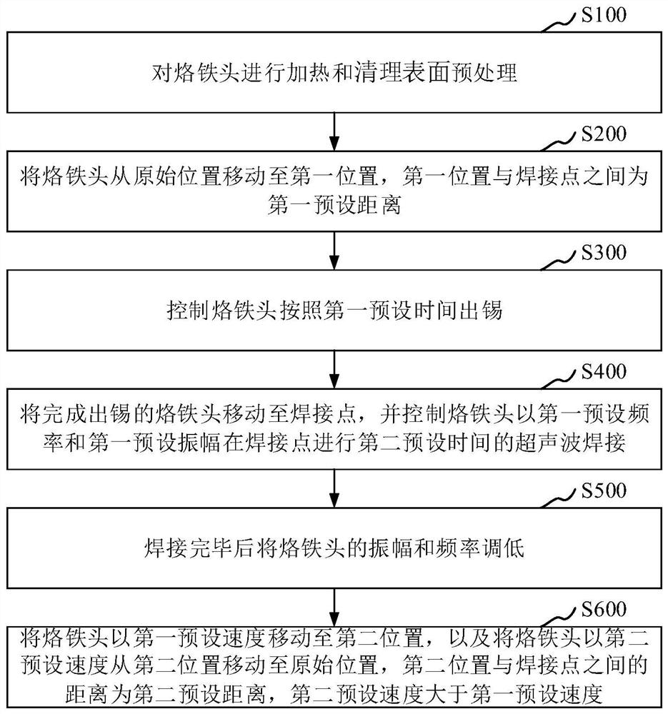
[0034] In one example, please refer to figure 1 As shown, the present invention provides a kind of circuit board welding method, and this method specifically comprises the following steps:

[0035] S100, pretreating the surface of the soldering iro...


PUM


Abstract

The invention discloses a circuit board welding method, a circuit board and electronic equipment. The method comprises the steps that heating and surface cleaning pretreatment are carried out on a soldering bit; the soldering bit is moved to a first position from the original position, and a first preset distance is formed between the first position and the welding point; the soldering bit is controlled to discharge tin according to a first preset time; The soldering bit completing tin discharging is moved to the welding point, and the soldering bit is controlled to carry out ultrasonic welding for a second preset time at the welding point at a first preset frequency and a first preset amplitude; after welding is completed, the amplitude and the frequency of the soldering bit are lowered;and the soldering bit is moved to the second position at the first preset speed, the soldering bit is moved to the original position from the second position at the second preset speed, the distance between the second position and the welding point is the second preset distance, and the second preset speed is larger than the first preset speed. According to the scheme, solder balls can be prevented from being generated, the production efficiency is improved, and the production cost is reduced.

Description

technical field [0001] The invention relates to the field of ultrasonic welding, in particular to a circuit board welding method, a circuit board and electronic equipment. Background technique [0002] Servers, computers, hard disks, GPUs, etc. contain various circuit board structures, and various components are welded on the circuit boards to achieve different functions. For example, thousands of electronic components are welded on the motherboard of servers and computers. These components often have strict requirements during the welding process. For example, in order to prevent the serial / parallel connection between components from being damaged or losing their original functions, solder balls cannot be produced during welding. ;In addition, solder balls are easy to vibrate randomly during the working process of the server and cause a short circuit on the motherboard. Due to the small size of such solder balls, it is difficult to find and clean them all during the solderi...

Claims


Application Information

Patent Timeline
Patent Type & Authority Applications(China)
IPC IPC(8): B23K3/00B23K3/08H05K3/34
CPCB23K3/00B23K3/08H05K3/34
Inventor 胡夕伦安妮
Owner INSPUR SUZHOU INTELLIGENT TECH CO LTD
Why Eureka
Try Eureka