Semiconductor process chamber

A process chamber and semiconductor technology, which is applied in the direction of metal material coating process, coating, gaseous chemical plating, etc., can solve the problems of poor uniformity of wafer coating, achieve uniform distribution of electric field intensity, good process results, and avoid Stronger effect

Active Publication Date: 2021-03-16
BEIJING NAURA MICROELECTRONICS EQUIP CO LTD
View PDF6 Cites 0 Cited by
  • Summary
  • Abstract
  • Description
  • Claims
  • Application Information

AI Technical Summary

Problems solved by technology

[0005] The present application discloses a semiconductor process chamber, which can solve the problem of poor uniformity of wafer coating

Method used


Image

  • Semiconductor process chamber
  • Semiconductor process chamber
  • Semiconductor process chamber

Examples


Embodiment Construction

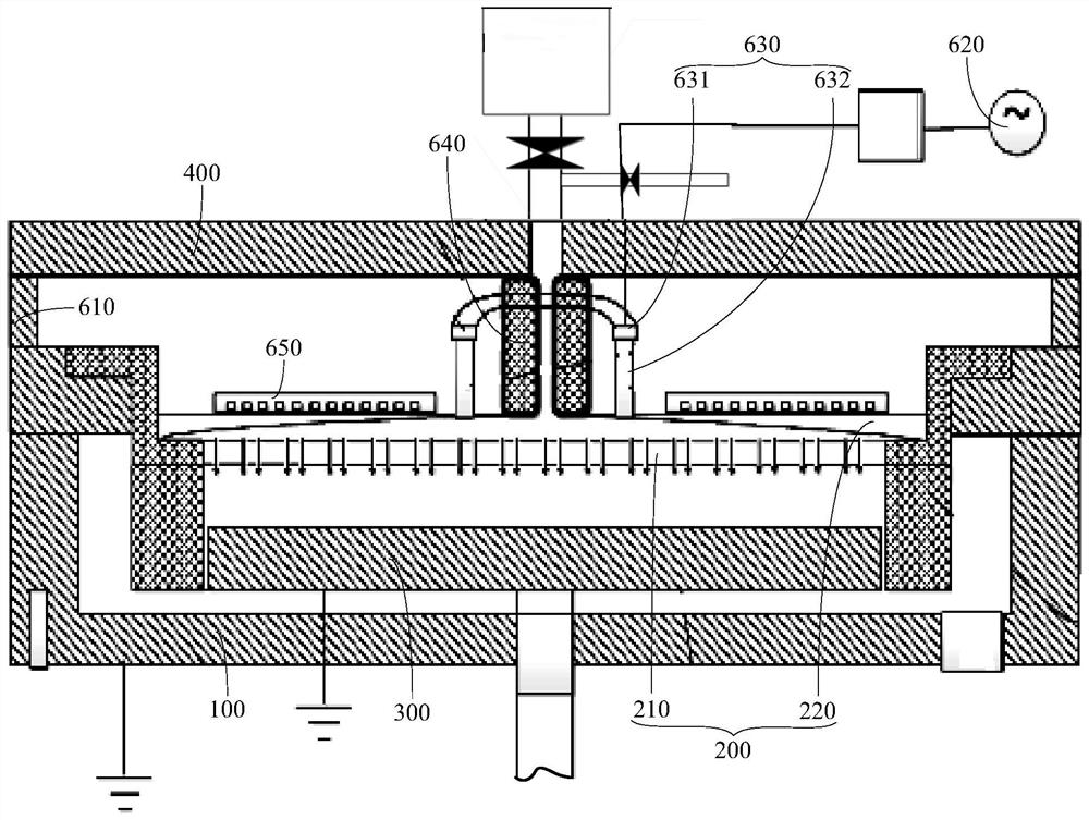
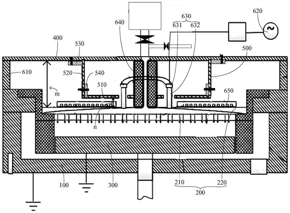
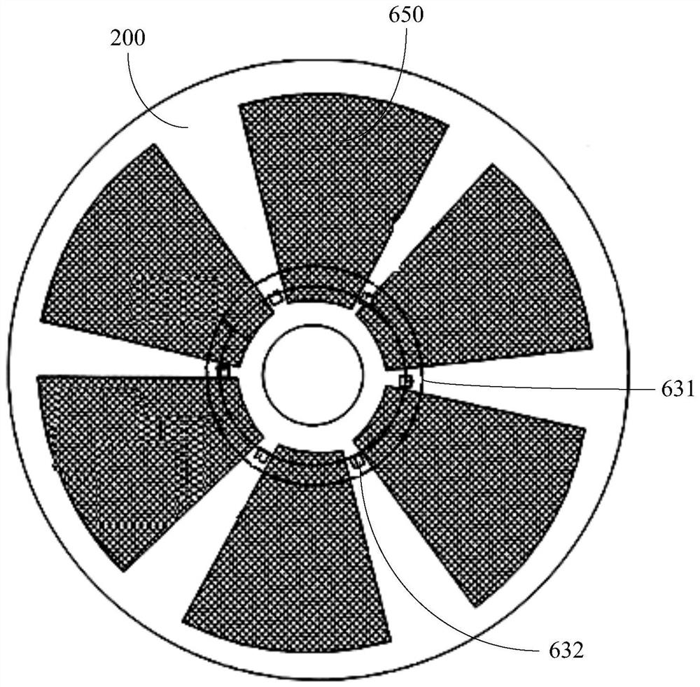
[0025] In order to make the purpose, technical solution and advantages of the present application clearer, the technical solution of the present application will be clearly and completely described below in conjunction with specific embodiments of the present application and corresponding drawings. Apparently, the described embodiments are only some of the embodiments of this application, not all of them. Based on the embodiments in this application, all other embodiments obtained by persons of ordinary skill in the art without making creative efforts belong to the scope of protection of this application.

[0026] The terms "first", "second" and the like in the specification and claims of the present application are used to distinguish similar objects, and are not used to describe a specific sequence or sequence. It is to be understood that the data so used are interchangeable under appropriate circumstances such that the embodiments of the application can be practiced in sequ...


PUM


Abstract

The invention discloses a semiconductor process chamber which comprises a chamber body, an upper electrode, a lower electrode, a shielding hood and an impedance adjusting mechanism, wherein the shielding hood is arranged on the chamber body and the shielding hood and the chamber body form an accommodation cavity, the upper electrode, the lower electrode and the impedance adjusting mechanism are arranged in the accommodation cavity, the upper electrode and the lower electrode are arranged oppositely, the upper electrode is located between the lower electrode and the shielding hood and is arranged in an electrically suspended manner, and the shielding hood and the lower electrode are earthed; the impedance adjusting mechanism is movably connected to the shielding hood and is electrically connected to the shielding hood, and the impedance adjusting mechanism can move far away from or close to the shielding hood to adjust the distance between the impedance adjusting mechanism and the upperelectrode; and / or, the impedance adjusting mechanism can move parallel to the shielding hood to change a relative area between the impedance adjusting mechanism and the upper electrode. According tothe scheme, the problem that the wafer coating uniformity is poor can be solved.

Description

technical field [0001] The present application relates to the technical field of semiconductor manufacturing, in particular to a semiconductor process chamber. Background technique [0002] In the semiconductor industry, as the geometries of electronic devices continue to shrink and the density of devices continues to increase, feature size and aspect ratio become more and more challenging. Atomic layer deposition (Atomic layer deposition, ALD) is a new thin film deposition method proposed to meet this challenge. With its unique self-limiting growth mode, atomic layer deposition has the advantages of precise and controllable film growth thickness, excellent shape retention, and controllable composition. It has attracted more and more attention from scientific and technological workers all over the world. [0003] In the prior art, the semiconductor process chamber mainly adopts the following two discharge modes: [0004] (1) The method of single-point feeding of the radio ...

Claims


Application Information

Patent Timeline
IPC IPC(8): C23C16/455C23C16/505C23C16/52
CPCC23C16/45544C23C16/505C23C16/52
Inventor 师帅涛
Owner BEIJING NAURA MICROELECTRONICS EQUIP CO LTD
Why Eureka
Try Eureka