Hemt device with sandwich gate dielectric structure and preparation method thereof
A gate dielectric and sandwich technology, applied in semiconductor devices, electrical components, circuits, etc., can solve the problems of device on-resistance and gate leakage current increase, device reliability reduction, electron scattering increase, etc., to achieve reduction Effects of gate leakage current, reduced electron concentration, and large threshold voltage
- Summary
- Abstract
- Description
- Claims
- Application Information
AI Technical Summary
Problems solved by technology
Method used
Image
Examples
Embodiment 1
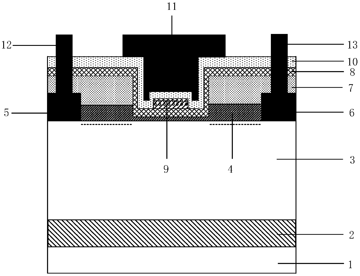
[0058] figure 2 It is a structural schematic diagram of a HEMT device with a sandwich gate dielectric structure provided by an embodiment of the present invention. Such as figure 2 As shown, the HEMT device with the sandwich gate dielectric structure provided by the embodiment of the present invention includes:
[0059] substrate1;
[0060] a buffer layer 2 on the substrate 1;
[0061] a GaN layer 3 on the buffer layer 2;
[0062] The barrier layer 4, the source electrode 5 and the drain electrode 6 located on the GaN layer 3, the barrier layer 4 has grooves on the side away from the GaN layer 3, and the barrier layer 4 has grooves on the source electrode 5 and the drain electrode 6. Between the poles 6, a heterojunction is formed between the GaN layer 3 and the barrier layer 4, and a heterojunction is formed at the interface, and the interface between the barrier layer 4 and the GaN layer 3 except the groove has a high-density 2DEG;
[0063] a passivation layer 7 locat...
Embodiment 2
[0078] Figure 4 The flow chart of the implementation of the fabrication method of the HEMT device with the sandwich gate dielectric structure provided by the embodiment of the present invention. Such as Figure 4 As shown, the preparation method of the HEMT device with the sandwich gate dielectric structure provided by the embodiment of the present invention includes:
[0079] Step 101, forming a laminated structure sequentially composed of a substrate, a buffer layer, a GaN layer and a barrier layer.
[0080] Figure 5a It is a structural diagram corresponding to this step in the method for manufacturing a HEMT device with a sandwich gate dielectric structure provided by an embodiment of the present invention. refer to Figure 5a , forming a laminated structure consisting of a substrate 1 , a buffer layer 2 , a GaN layer 3 and a barrier layer 4 in sequence. A substrate 1 is provided; a buffer layer 2 is formed on the substrate 1 ; a GaN layer 3 is formed on the buffer l...
PUM
 Abstract
Description
Claims
Application Information


