Semiconductor device
A semiconductor and conductive type technology, applied in the direction of semiconductor devices, electric solid devices, electrical components, etc., can solve the problem of increased on-resistance
- Summary
- Abstract
- Description
- Claims
- Application Information
AI Technical Summary
Problems solved by technology
Method used
Image
Examples
no. 1 Embodiment approach
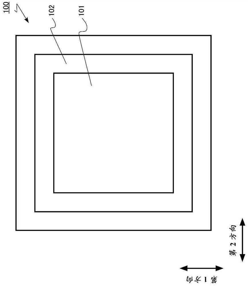
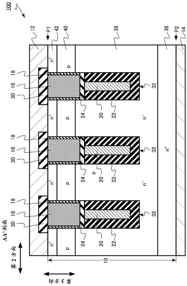
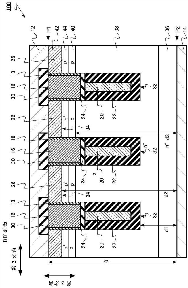
[0028] The semiconductor device according to the first embodiment includes: a semiconductor layer having a first surface and a second surface facing the first surface; Extending in the first direction; the second groove, located on the side of the first surface, extending in the second direction perpendicular to the first direction, intersecting the first groove; the first semiconductor region of the first conductivity type; the second groove The second semiconductor region of the 2 conductivity type is located between the first semiconductor region and the first surface; and the third semiconductor region of the first conductivity type is located between the second semiconductor region and the first surface; the gate electrode is located on the first surface In the trench; the field plate electrode, in the first trench, is located between the gate electrode and the second surface; the metal region, located in the second trench, is electrically connected to the second semicondu...
no. 2 Embodiment approach
[0093] The semiconductor device according to the second embodiment differs from the first embodiment in that the first thickness of the gate insulating layer between the gate electrode and the semiconductor layer is thinner than the second thickness of the gate insulating layer between the gate electrode and the metal region. Different types of semiconductor devices. In addition, the semiconductor device according to the second embodiment differs from the first embodiment in that the width in the second direction of the portion of the gate electrode facing the semiconductor layer is greater than the width in the second direction of the portion of the gate electrode facing the metal region. different semiconductor devices. Hereinafter, descriptions may be partially omitted regarding content that overlaps with the semiconductor device of the first embodiment.
[0094] The semiconductor device according to the second embodiment is a vertical transistor in which a gate electrode ...
no. 3 Embodiment approach
[0108] The semiconductor device of the third embodiment differs from the semiconductor device of the first embodiment in that the gate electrode has a first region and a second region separated from each other in the second direction in the first trench. Hereinafter, descriptions may be partially omitted regarding content that overlaps with the semiconductor device of the first embodiment.
[0109] The semiconductor device according to the third embodiment is a vertical transistor in which a gate electrode is buried in a trench. The semiconductor device of the third embodiment is a vertical power MOSFET. The semiconductor device of the third embodiment is a MOSFET 300 .
[0110] Figure 11 It is a schematic cross-sectional view of the semiconductor device of the third embodiment. Figure 11 is the same as the first embodiment figure 2 corresponding figure.
[0111] Figure 12 It is a schematic plan view of the semiconductor device of the third embodiment. Figure 12 is...
PUM
 Abstract
Description
Claims
Application Information
 - R&D Engineer
- R&D Manager
- IP Professional
- Industry Leading Data Capabilities
- Powerful AI technology
- Patent DNA Extraction
Browse by: Latest US Patents, China's latest patents, Technical Efficacy Thesaurus, Application Domain, Technology Topic, Popular Technical Reports.
© 2024 PatSnap. All rights reserved.Legal|Privacy policy|Modern Slavery Act Transparency Statement|Sitemap|About US| Contact US: help@patsnap.com


