Supercharge Your Innovation With Domain-Expert AI Agents!

Semiconductor structure and manufacturing and thinning method thereof

A semiconductor and substrate technology, which is applied in the fields of thinning, semiconductor structures and their fabrication, and can solve problems such as low efficiency and poor chip quality.

Pending Publication Date: 2021-03-19
GUANGDONG INST OF SEMICON IND TECH
View PDF7 Cites 0 Cited by
  • Summary
  • Abstract
  • Description
  • Claims
  • Application Information

AI Technical Summary

Problems solved by technology

[0004] The purpose of this application is to provide a semiconductor structure and its manufacturing and thinning methods to solve the problems of poor quality and low efficiency when thinning chips in the prior art

Method used


Image

  • Semiconductor structure and manufacturing and thinning method thereof
  • Semiconductor structure and manufacturing and thinning method thereof
  • Semiconductor structure and manufacturing and thinning method thereof

Examples


no. 1 example

[0039] As mentioned in the background technology, most of the existing chip thinning methods are mechanical grinding, that is, using a thinning machine or a polishing machine for thinning. The thinning thickness is greatly restricted by the equipment, and, due to the , The transistor circuit and wiring are more complex, resulting in uneven stress, so after mechanical grinding, the obtained chips are of poor quality. At the same time, the efficiency of mechanical grinding is also low.

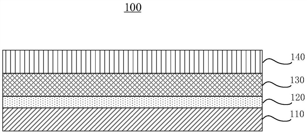
[0040] In view of this, in order to solve the above problems, the present application provides a semiconductor structure, by setting a thinned functional layer in the semiconductor structure, and the etching rate of the substrate and the target etching solution is greater than or equal to the thinned functional layer 2 times the etching rate of the target etching solution. So that when the semiconductor structure is placed in the target etching solution, after the substrate and the buffer layer...

no. 2 example

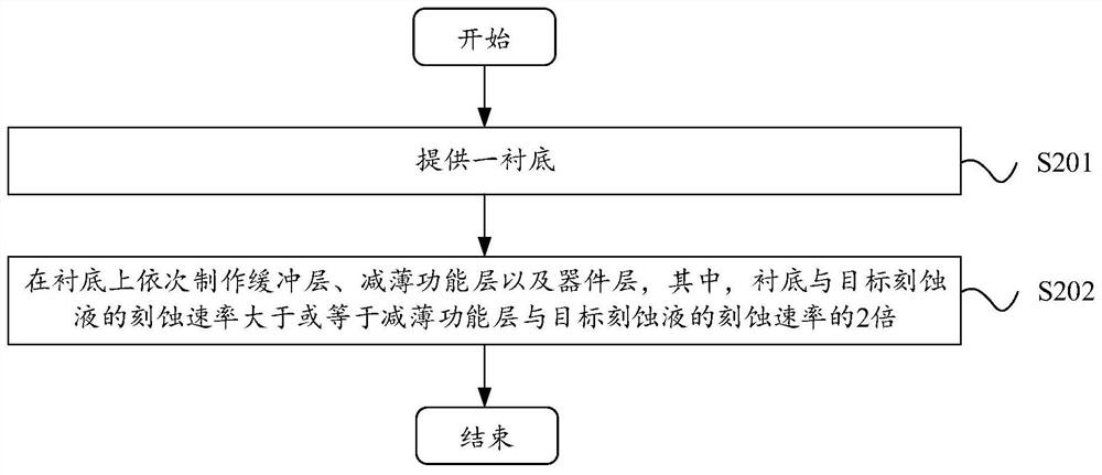
[0055] see figure 2 , the embodiment of the present application also provides a semiconductor structure manufacturing method, the semiconductor structure manufacturing method can manufacture the semiconductor structure described in the first embodiment, the method includes:

[0056] S201, providing a substrate.

[0057] S202, sequentially fabricating a buffer layer, a thinned functional layer and a device layer on the substrate, wherein the etching rate of the substrate and the target etching solution is greater than or equal to 2 of the etching rate of the thinned functional layer and the target etching solution times.

[0058] Wherein, the material of the thinned functional layer and the substrate can be any one of the materials described in the first embodiment, which is not limited in this application.

[0059] In addition, in this application, there is no limitation on the production process of the thinned functional layer, which can be produced by epitaxial process or...

no. 3 example

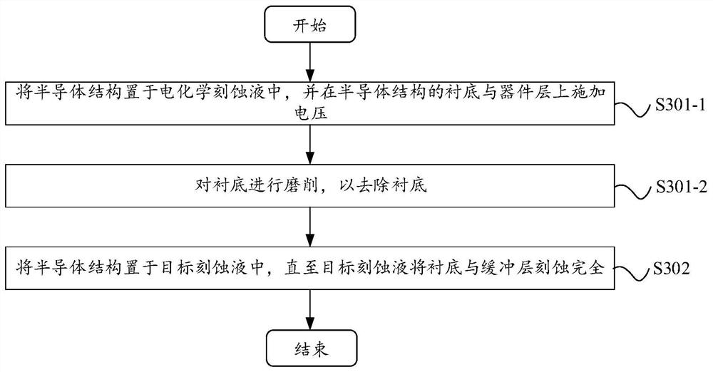
[0061] see image 3 , the embodiment of the present application also provides a semiconductor structure thinning method, which can be used to thin the semiconductor structure described in the first embodiment. As an optional implementation, the method includes:

[0062] S302, placing the semiconductor structure in a target etchant until the target etchant completely etches the substrate and the buffer layer.

[0063] That is, in this application, chemical etching is used to thin the semiconductor structure, and the material of the target etching solution has been described in detail in the first embodiment, and will not be repeated here.

[0064] It can be understood that in fabricating the semiconductor structure, since the front and side surfaces of the device layer are encapsulated, it is possible to isolate the target etchant from etching the device material. When the semiconductor structure is placed in the target etchant, the target etchant can etch away the sinker and...


PUM

PropertyMeasurementUnit
thicknessaaaaaaaaaa
thicknessaaaaaaaaaa
thicknessaaaaaaaaaa

Abstract

The invention provides a semiconductor structure and a manufacturing and thinning method thereof, and relates to the technical field of semiconductor material processing. The semiconductor structure comprises a substrate, a buffer layer, a thinning function layer and a device layer, wherein the substrate, the buffer layer, the thinning function layer and the device layer are connected layer by layer; and the etching rate of the substrate and the target etching liquid is greater than or equal to two times of the etching rate of the thinning function layer and the target etching liquid. The semiconductor structure and the manufacturing and thinning method thereof provided by the invention have the effects of high thinning efficiency and better quality.

Description

technical field [0001] The present application relates to the technical field of semiconductor material processing, in particular, to a semiconductor structure and its manufacturing and thinning methods. Background technique [0002] In recent years, with the development of network technology, electronic equipment and instruments are required to have multiple functions, high reliability, small size, and portability, and the requirements for device dimensions are getting smaller and smaller. The miniaturization requirements of device dimensions, the improvement of packaging structure, and the development and progress in various aspects such as reducing thermal resistance and improving the heat dissipation capacity of chips. Correspondingly, the chips used for packaging are required to be thinner and thinner, and the quality is higher and higher. In many emerging areas of semiconductor manufacturing, ultra-thin chips are required. In these fields, the development trend of ul...

Claims


Application Information

Patent Timeline
Patent Type & Authority Applications(China)
IPC IPC(8): H01L21/306H01L21/304
CPCH01L21/30604H01L21/304
Inventor 胡川卢瀚仑陈志涛王垚
Owner GUANGDONG INST OF SEMICON IND TECH
Features
  • R&D
  • Intellectual Property
  • Life Sciences
  • Materials
  • Tech Scout
  • Unparalleled Data Quality
  • Higher Quality Content
  • 60% Fewer Hallucinations
Learn More