Raw material cleaning and decontaminating device for photoelectronic device production

A technology of optoelectronic devices and raw materials, applied in the field of optoelectronics, can solve problems such as lack of cleaning devices

Inactive Publication Date: 2021-03-26
WEST ANHUI UNIV
View PDF6 Cites 3 Cited by
  • Summary
  • Abstract
  • Description
  • Claims
  • Application Information

AI Technical Summary

Problems solved by technology

[0003] The raw materials used in the production process of optoelectronic devices are generally processed through multiple processes, and ...

Method used


Image

  • Raw material cleaning and decontaminating device for photoelectronic device production
  • Raw material cleaning and decontaminating device for photoelectronic device production
  • Raw material cleaning and decontaminating device for photoelectronic device production

Examples


Embodiment 1

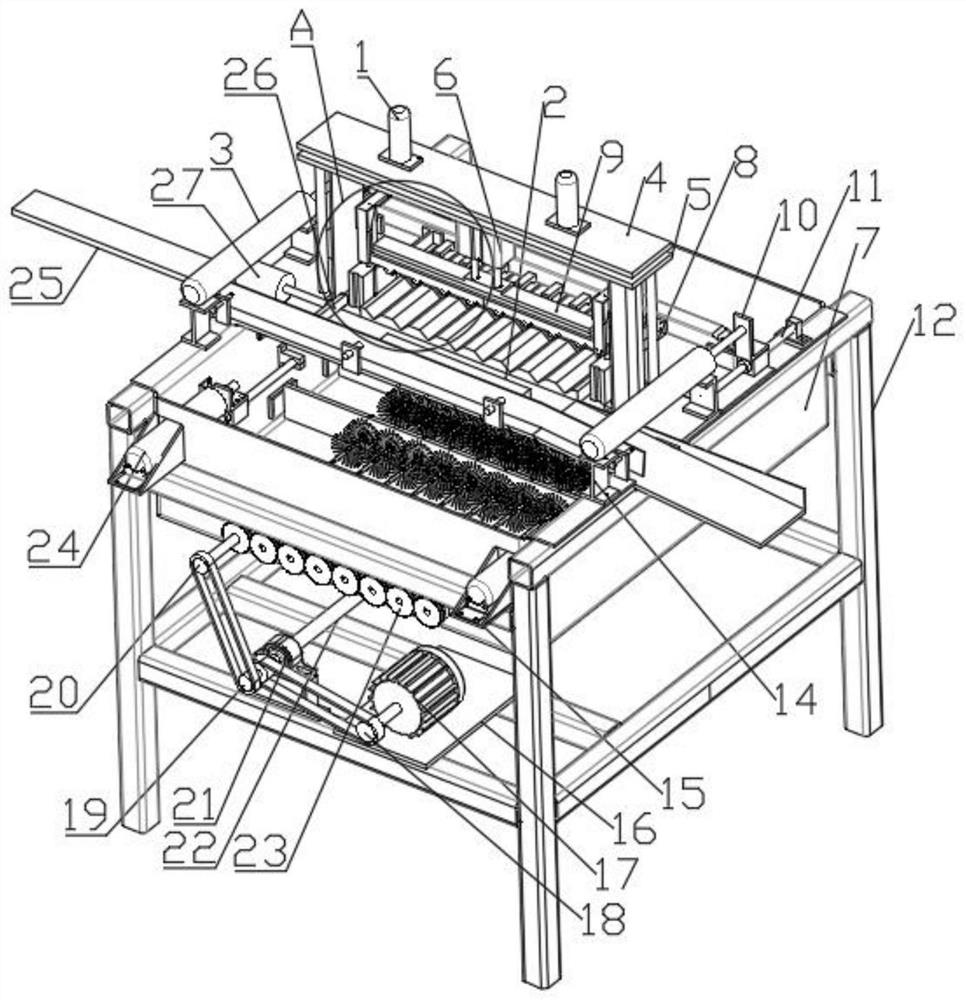
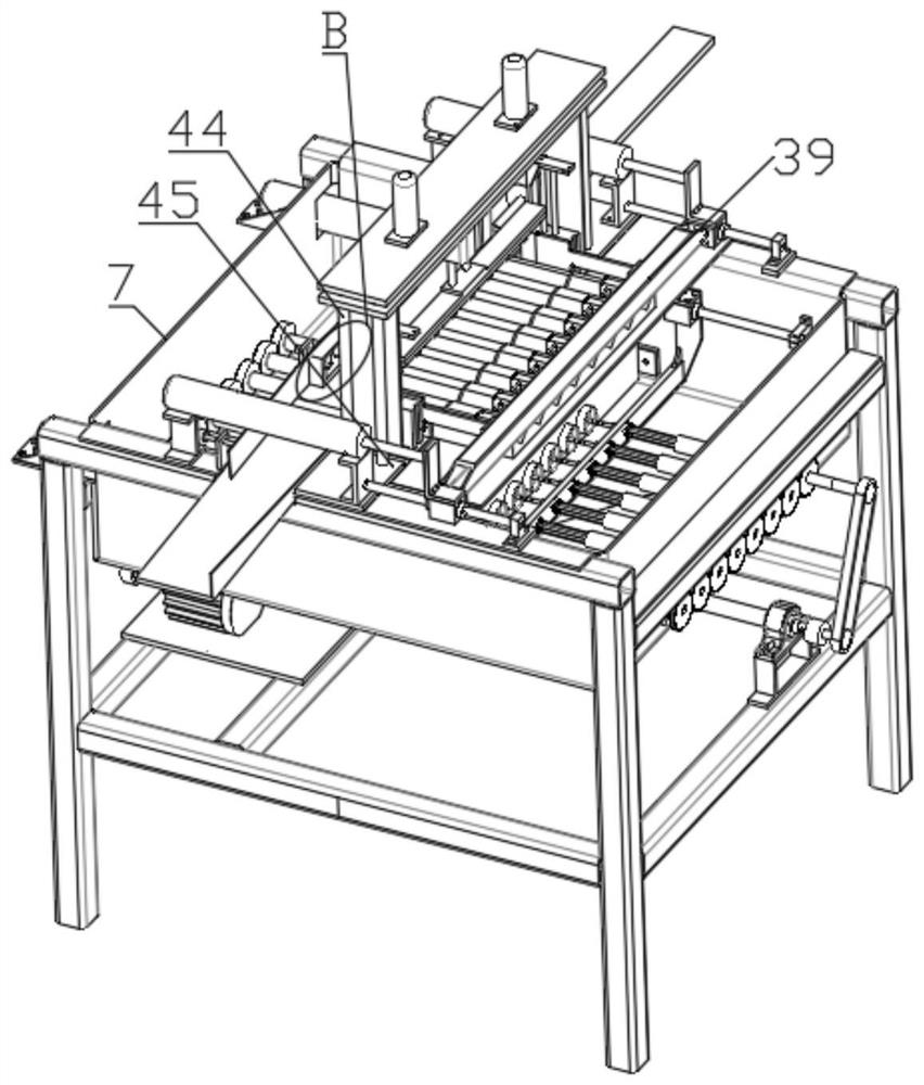
[0027] see Figure 1-6 , in an embodiment of the present invention, a raw material cleaning and decontamination device for optoelectronic device production mainly includes a mounting frame 12 .

[0028] The upper side crossbeam of described installation frame 12 is divided into left crossbeam and right crossbeam, and water tank 7 is arranged between described left crossbeam and right crossbeam, and the upper side of described water tank 7 is provided with feeding chute 25, and described feeding trough No. 5 telescopic motor 27 and scraping box 2 are arranged on the upper side of 25. A plurality of friction rollers 13 are arranged in the scraping box 2. A layer of water-absorbent cotton material, the telescopic part of the No. 5 telescopic motor 27 is connected with a support plate 26, the left beam and the right beam are all provided with a receiving plate 45, and the upper side of the receiving plate 45 is provided with a plurality of No. 1 Guide rod 8, on the No. 1 guide ro...

Embodiment 2

[0033] On the basis of the raw material cleaning and decontamination device for optoelectronic device production described in embodiment 1, the differences between this embodiment and embodiment 1 are:

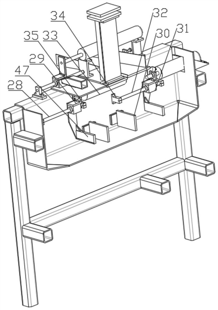
[0034] In this embodiment, a plurality of baffles 30 are fixedly connected between the left and right inner walls of the water tank 7, and a plurality of guide sleeves 36 are sleeved on the baffles 30, and the guide sleeves 36 have elastic Plastic material, two sets of brushes 38 are arranged between the two adjacent baffle plates 30, and the back-to-back ends of the adjacent two brushes 38 are connected with connecting rods 40, the connecting rods 40 The radius is smaller than the opening radius of the guide sleeve 36, and the other end of the connecting rod 40 is connected with a strut, and the strut is fixedly connected with the transverse splint 47 and the strut is connected with the transverse splint 47, and the other end of the strut is connected There is a rotating rod ...


PUM


Abstract

The invention relates to the field of optoelectronics, in particular to a raw material cleaning and decontaminating device for photoelectronic device production. The raw material cleaning and decontaminating device comprises a mounting frame, wherein an upper cross beam of the mounting frame is divided into a left cross beam and a right cross beam, a water tank is arranged between the left cross beam and the right cross beam, and a plurality of baffles are fixedly connected between the inner walls of the left side and the right side of the water tank; the baffles are sleeved with a plurality of guide sleeves, and the guide sleeves are made of elastic plastic materials; two brushes are arranged between every two front-back adjacent baffles, the ends, opposite to each other, of every two adjacent brushes are connected with connecting rods, and the radius of each connecting rod is smaller than that of an open hole of the corresponding guide sleeve; and the other ends of the connecting rods are connected with supporting rods, and the supporting rods penetrate through transverse clamping plates and are fixedly connected with the transverse clamping plates. The raw material cleaning anddecontaminating device for photoelectronic device production is scientific in structure, and raw materials for electronic equipment production can be deeply cleaned, so that adverse effects of impurities on subsequent production are avoided.

Description

technical field [0001] The invention relates to the field of optoelectronics, in particular to a device for cleaning and decontaminating raw materials used in the production of optoelectronic devices. Background technique [0002] Optoelectronics refers to electronics in the light wave band, namely infrared, visible light, ultraviolet and soft X-ray (frequency range 3×10¹¹Hz~3×10¹⁶Hz or wavelength range 1mm~10nm). After the cross-penetration of optoelectronic technology and its related technologies in the 1980s, its technology and applications have achieved rapid development in the 1990s, playing an increasingly important role in social informationization. [0003] The raw materials used in the production process of optoelectronic devices are generally processed through multiple processes, and their surfaces are often contaminated with many sticky substances, and such sticky substances often lack effective cleaning devices to clean them. [0004] Therefore, in view of the a...

Claims


Application Information

Patent Timeline
IPC IPC(8): B08B1/04B08B3/04B08B13/00F26B5/14
CPCB08B1/002B08B1/04B08B3/04B08B13/00F26B5/14
Inventor 刘向远方杰杜成涛孔敏程宝安
Owner WEST ANHUI UNIV
Why Eureka
Try Eureka