

A method for identifying nanostructures of thin film materials based on ellipsometry parameter trajectory topological features
A thin-film material and nanostructure technology, applied in nanomaterials and optics, which can solve problems such as harsh environmental requirements, probe damage, pollution, etc.
Active Publication Date: 2021-09-17
FUDAN UNIV
View PDF0 Cites 0 Cited by
- Summary
- Abstract
- Description
- Claims
- Application Information
AI Technical Summary
Problems solved by technology
Field emission scanning electron microscopy and transmission electron microscopy have harsh environmental requirements, both require a vacuum environment, have requirements on the size of the sample, and damage the sample during the test
In addition, sample preparation for TEM testing is complex and expensive
The atomic force microscope has inherent shortcomings. In the case of improper operation or contamination on the sample surface, it is very easy to damage or contaminate the probe due to the striker, and the damage or contamination of the probe greatly affects the quality of the image.
During the measurement process, the scanning speed of the probe is very slow, which greatly reduces the work efficiency
Method used
View moreImage
Smart ImageViewing Examples

Examples
Embodiment
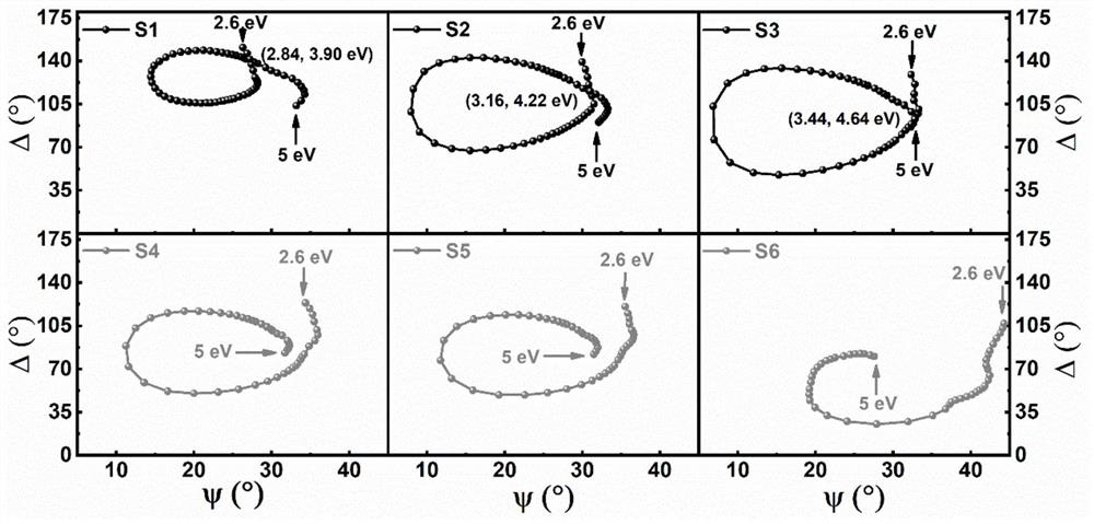
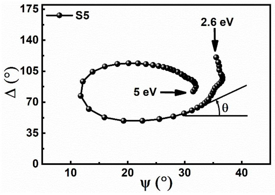
[0040] This example describes the specific implementation of the present invention by identifying the nanostructure of silver thin film.
[0041] Silver thin films with different nanostructures were prepared on silicon substrates by electron beam evaporation.
Login to View More PUM
 Abstract
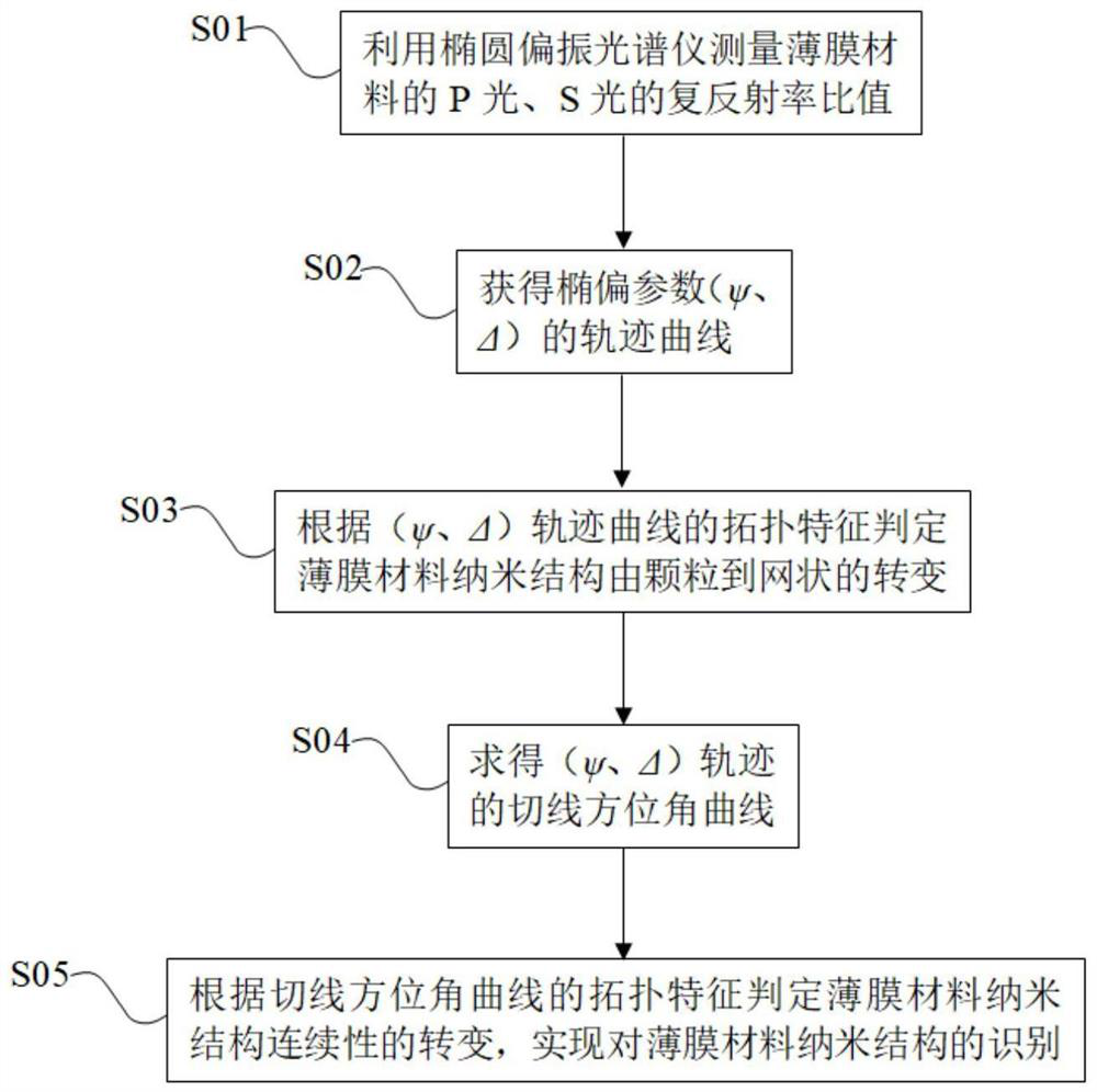
The invention belongs to the field of nanometer material and optical technology, and specifically relates to a method for identifying the nanostructure of thin film material based on the topological feature of ellipsometric parameter trajectory. The method of the present invention comprises the following steps: Utilize the spectroscopic ellipsometer to measure the complex reflectance ratio ρ of the P light and the S light of the film material, and then obtain two ellipsometric parameters ψ and Δ; obtain the locus curve of the ellipsometric parameters (ψ, Δ) ; According to the topological characteristics of the trajectory curve, the transition of the film material nanostructure from particle to network is determined; the tangent azimuth angle curve of the (ψ, Δ) trajectory is obtained; the film material nanostructure is determined according to the topological characteristics of the tangent azimuth curve The transformation of the structural continuity enables the recognition of the nanostructure of thin film materials. The invention can be used for in-situ monitoring of nanostructures in the growth process of thin film materials, has important reference value for using artificial intelligence to identify nanostructures, and has the advantages of non-contact, non-destructive, and less demanding on the environment.
Description
technical field [0001] The invention belongs to the field of nanometer material and optical technology, and in particular relates to an identification method of nanostructure of thin film material. Background technique [0002] Thin film materials have special properties that traditional bulk materials do not have, so they are widely used in microelectronics, optoelectronics and other fields. The application of thin film materials in different fields is closely related to their nanostructures. Therefore, studying the nanostructure of thin film materials can develop more potential applications. [0003] At present, the technical methods for characterizing the nanostructure of thin film materials mainly include field emission scanning electron microscopy, transmission electron microscopy and atomic force microscopy. Field emission scanning electron microscopy and transmission electron microscopy have harsh requirements on the environment, both of which require a vacuum envir...
Claims
Login to View More Application Information
Patent Timeline
 Patent Type & AuthorityPatents(China)
IPC IPC(8): G01N21/21
CPCG01N21/211G01N2021/213
Inventor刘翩郑玉祥陈良尧张荣君王松有李晶杨月梅
OwnerFUDAN UNIV