A chip input buffer circuit and memory

An input buffer circuit and chip technology, applied in the semiconductor field, can solve the problems of increasing the chip area of ​​the charge pump, unfavorable chip packaging, etc.

Active Publication Date: 2022-06-21
WUHAN XINXIN SEMICON MFG CO LTD
View PDF8 Cites 0 Cited by
  • Summary
  • Abstract
  • Description
  • Claims
  • Application Information

AI Technical Summary

Problems solved by technology

Therefore, using the charge pump inside the chip to generate HV for CP testing requires increasing the chip area occupied by the charge pump, which is not conducive to chip packaging.

Method used


Image

  • A chip input buffer circuit and memory
  • A chip input buffer circuit and memory
  • A chip input buffer circuit and memory

Examples


Embodiment Construction

[0016] The technical solutions in the embodiments of the present application will be clearly and completely described below with reference to the accompanying drawings in the embodiments of the present application. Obviously, the described embodiments are only a part of the embodiments of the present application, but not all of the embodiments. Based on the embodiments in the present application, all other embodiments obtained by those skilled in the art without creative work fall within the protection scope of the present application. The same or similar reference numbers throughout the embodiments denote the same or similar elements or elements having the same or similar functions.

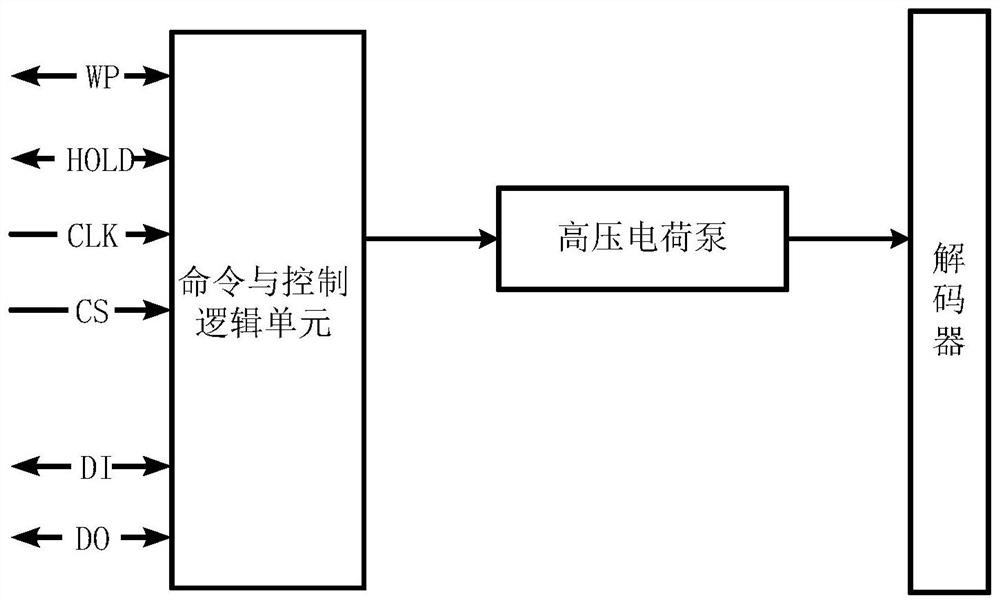
[0017] An input buffer is an indispensable basic block in an integrated circuit, and it can be configured to perform voltage detection for a threshold voltage in order to confirm whether the voltage of the input signal is higher or lower than the threshold voltage. An input buffer consisting of...


PUM


Abstract

The application discloses a chip input buffer circuit and memory. The chip input buffer circuit of this application, by using the pads of the chip itself, adds a high-voltage path in the original chip input buffer circuit, and performs logical control on the original data path; in the test mode, the pads of the chip itself can be used to The external high-voltage signal is output to the internal high-voltage path of the chip to meet the high-voltage requirements of chip testing, and to provide the internal data signal of the first level to the internal data path of the chip; in normal working mode, the internal high-voltage signal is output to the internal high-voltage path, and provide normal levels of internal data signals to the internal data path.

Description

technical field [0001] The present application relates to the field of semiconductor technology, and in particular, to a chip input buffer circuit and a memory capable of realizing chip testing. Background technique [0002] Semiconductor chips are the core components in the electronics industry. Due to process deviations in the production process of the chips, it is necessary to test chip-by-chip at the wafer level, and reject the chips that do not meet the requirements. Chip testing (Chip Probe, CP for short) is generally performed by changing the working voltage of the chip. The CP test needs to complete the chip functional test as fast as possible to reduce the cost, which means that there are more dies (die) to be tested at the same time than normal, and the test operation is also required to be faster. Therefore, it is necessary to provide a higher high voltage power supply (HV) to the chip during CP testing. [0003] Currently, there are two ways to generate HV for ...

Claims


Application Information

Patent Timeline
Patent Type & Authority Patents(China)
IPC IPC(8): G11C7/10G11C5/14G11C29/12G11C29/56
CPCG11C7/1084G11C5/147G11C29/56G11C29/12G11C5/145G11C29/12005
Inventor 赵慧超
Owner WUHAN XINXIN SEMICON MFG CO LTD
Why Eureka
Try Eureka