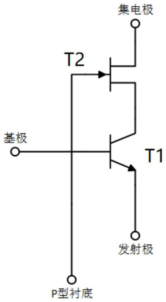
High-voltage NPN device
A device and high-voltage technology, which is applied in the field of high-voltage NPN devices, can solve problems such as increased spacing, poor cost performance, and increased device size, and achieve the effects of simplifying the manufacturing process, improving product cost performance, and meeting high-voltage resistance requirements
- Summary
- Abstract
- Description
- Claims
- Application Information
AI Technical Summary
Problems solved by technology
Method used
Image

Examples
Embodiment 1
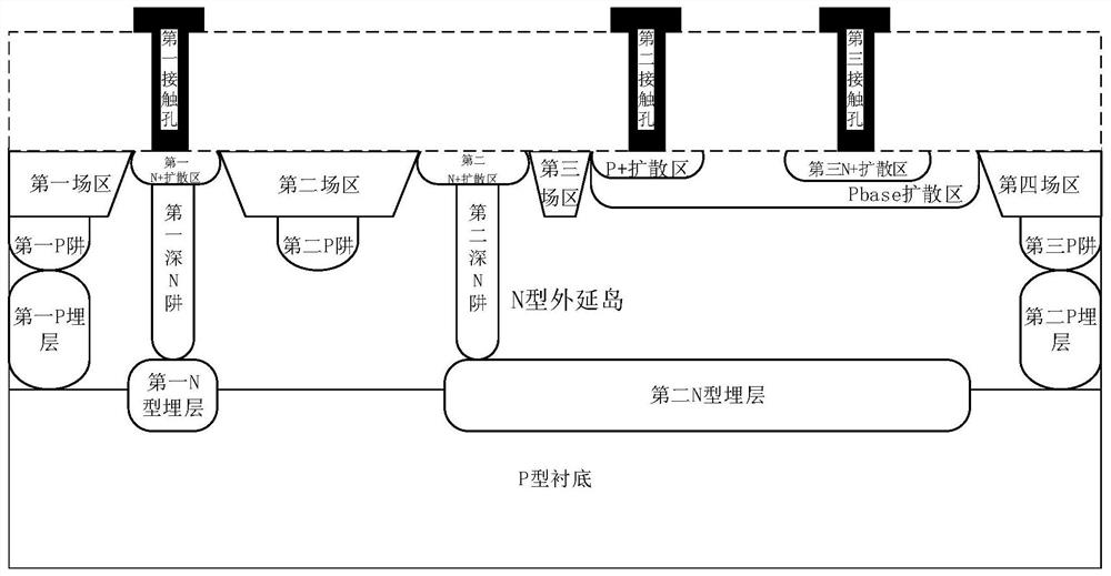
[0043] Such as figure 2 As shown, an N-type epitaxial island is provided above the P-type substrate, and between the lower end of the N-type epitaxial island and the P-type substrate, a first N-type buried layer and a second N-type buried layer are arranged in sequence from left to right. buried layer;
[0044] The top of the first N-type buried layer is sequentially connected to the first deep N well diffusion region and the first N+ diffusion region from bottom to top, and an ohmic contact is formed above the first N+ diffusion region through a contact hole and a metal line, as the JFET The drain of the tube and the collector terminal of the high-voltage NPN device;
[0045] The N-type epitaxial island is provided with a second P well region, the second P well region is located above the first N-type buried layer and the second N-type buried layer, and the second P well region Connected to the P-type substrate directly below it as the gate of the JFET tube;
[0046] The ...
Embodiment 2
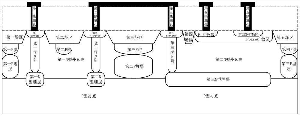
[0054] Such as image 3 As shown, a first N-type epitaxial island and a second N-type epitaxial island are arranged adjacent to each other from left to right above the P-type substrate, and between the lower end of the first N-type epitaxial island and the P-type substrate A first N-type buried layer and a second N-type buried layer are sequentially provided from left to right; a third N-type buried layer is provided between the lower end of the second N-type epitaxial island and the P-type substrate;
[0055] The top of the first N-type buried layer is sequentially connected to the first deep N well diffusion region and the first N+ diffusion region from bottom to top, and an ohmic contact is formed above the first N+ diffusion region through a contact hole and a metal line, as the JFET The drain of the tube and the collector terminal of the high-voltage NPN device;
[0056] The first N-type epitaxial island is provided with a second P well region, the second P well region i...
Embodiment 3
[0065] Such as Figure 4 As shown, the difference between the third embodiment and the second embodiment mainly lies in that there is a space between the first N-type epitaxial island and the second N-type epitaxial island, and other components can be arranged in the space. Although this will increase the device area, it increases the flexibility of the layout layout, and the characteristics of the high-voltage NPN device composed of it remain unchanged.
PUM
 Abstract
Description
Claims
Application Information
 - R&D
- Intellectual Property
- Life Sciences
- Materials
- Tech Scout
- Unparalleled Data Quality
- Higher Quality Content
- 60% Fewer Hallucinations
Browse by: Latest US Patents, China's latest patents, Technical Efficacy Thesaurus, Application Domain, Technology Topic, Popular Technical Reports.
© 2025 PatSnap. All rights reserved.Legal|Privacy policy|Modern Slavery Act Transparency Statement|Sitemap|About US| Contact US: help@patsnap.com