Semiconductor device unit, manufacturing method thereof and forming device

A manufacturing method and semiconductor technology, applied in the direction of semiconductor devices, semiconductor/solid-state device manufacturing, transistors, etc., can solve the problem that the entire device loses its function

Pending Publication Date: 2021-03-30
GLOBAL ENERGY INTERCONNECTION RES INST CO LTD +2
View PDF3 Cites 0 Cited by
  • Summary
  • Abstract
  • Description
  • Claims
  • Application Information

AI Technical Summary

Problems solved by technology

[0007] In order to solve the problem in the prior art that the control edge of the insulating gate needs to bear stress, and the whole device will lose its function when there is a problem with the...

Method used


Image

  • Semiconductor device unit, manufacturing method thereof and forming device
  • Semiconductor device unit, manufacturing method thereof and forming device
  • Semiconductor device unit, manufacturing method thereof and forming device

Examples


Embodiment 1

[0069] A semiconductor device comprising: at least one unit;

[0070] Each unit includes:

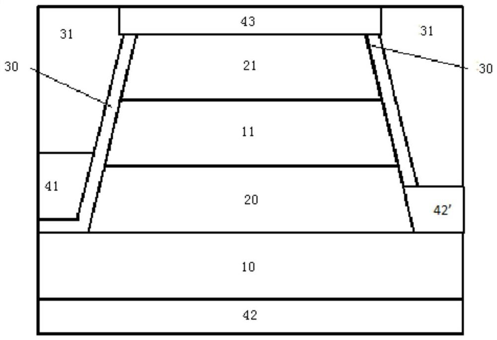
[0071] Such as image 3 As shown, the semiconductor substrate material used as the support layer forms the collector region 10 and has a first doping characteristic;

[0072] The semiconductor layer with the second doping characteristic located on the collector region 10 forms a drift region 20;

[0073] A semiconductor layer with a first doping characteristic located above the drift region 20 forms a well region 11;

[0074] The semiconductor layer with the second doping characteristic located above the well region 11 forms an emitter region 21;

[0075] The insulating layer covering the sides of the collector region 10, the drift region 20, the well region 11, and the emitter region 21 forms an insulating gate 30, which may be silicon oxide or other insulating layers;

[0076] The conductive layer on the insulating gate 30 forms the gate electrode 41, which may be doped polysilico...


PUM


Abstract

The invention provides a semiconductor device unit and a manufacturing method and a forming device thereof. The unit comprises a laminated layer formed by stacking semiconductor material layers with two doping characteristics, a gate control structure and an insulating passivation layer (31); the laminated layer is of a boss structure, wherein the upper bottom face is smaller than the lower bottomface, and the side face of the boss is of a positive oblique angle or right angle structure. The insulating passivation layer (31) is arranged on the side surface of the laminated layer and is matched with the positive bevel angle or right angle structure to form a cubic structure with the laminated layer; the gate control structure is provided between the insulating passivation layer (31) and the stacked layer. According to the invention, the stress surface is smooth, the stress is uniform, the stress of the insulated gate is small, and large-area interconnection can be realized.

Description

technical field [0001] The invention relates to the field of semiconductors, in particular to a semiconductor device unit, a manufacturing method thereof and a device formed therein. Background technique [0002] Semiconductor devices based on semiconductor materials usually achieve specific functions by including P-type and N-type PN junctions or by including metal-semiconductor Schottky junctions and metal-oxide-semiconductor gate control structures. Features. These structures are often achieved by local doping or thin-film processes. Semiconductor devices use these structures to control current on and off, thereby realizing signal transmission. For high-power applications, semiconductor devices are often required to have the ability to block high voltage and conduct high current at the same time. However, in order to realize these functions, it is necessary to effectively reduce the on-resistance of the semiconductor material, and to effectively isolate the termination...

Claims


Application Information

Patent Timeline
IPC IPC(8): H01L29/06H01L29/423H01L29/739H01L21/28H01L21/331
CPCH01L29/0649H01L29/0657H01L29/0684H01L29/401H01L29/42356H01L29/66333H01L29/7397H01L29/7398
Inventor 查祎英金锐董少华王耀华桑玲吴军民潘艳
Owner GLOBAL ENERGY INTERCONNECTION RES INST CO LTD
Why Eureka
Try Eureka