Capacitance detection circuit, touch chip and electronic equipment
A capacitance detection and capacitance detection technology, applied in electronic switches, electrical components, electrical digital data processing, etc., can solve the problems of low sensitivity, small capacitance change, and circuit noise flooding, etc. The effect of accuracy
Active Publication Date: 2022-06-07
SHENZHEN GOODIX TECH CO LTD
4 Cites 0 Cited by
AI-Extracted Technical Summary
Problems solved by technology
A small capacitance change means that a higher circuit gain is required so that the detection circuit can detect the electrical signal generated by the capacitance change when touched, but since the basic capacitance is much higher than the capacitance change, if a higher circuit is used Gain can easily cause the detection circuit to saturat...
Method used
[0055] Optionally, during implementation, the drive module may include at least two switch units, and the at least two switch units switch switch states under the control of the control module to form the first charging branch Or the second charging branch can eliminate low-frequency noise in the circuit and improve the signal-to-noise ratio. In the following embodiments, the driving module includes two switch units as an example for illustration.
[0075] Optionally, in this embodiment, it is set that the resistance value of the first offset resistor is not equal to the resistance value of the second offset resistor. Since the charging and discharging speeds of the circuit are different, by setting the size of the first offset resistor to be different from the size of the second offset resistor, the voltage on the detection capacitor is exactly Vcm when there is no touch operation, so as to achieve perfect offset. To improve the sensitivity of touch detection.
[0102] Optionally, in this embodiment, the size of R1 is set to be unequal to the size of R2. Since the speed of charging and discharging the circuit is different, the size of R1 is set to be unequal to the size of R2, so that there is no touch operation When , the voltage on the detection capacitor is exactly Vcm, so as to achieve perfect offset to improve the sensitivity of touch detection.
[0103] Considering that t1-t3 and t4-t6 are symmetrical processes, t1 and t4, t3 and t6 will be set to be the same, so it is expected that the values of t2 and t5 are also the same or close to each other. According to the operating frequency of the circuit, first determine the target values of t2 and t5, and then determine the calculated values of resistors R1 and R2 according to the values of Vcc, Vss, Vcm and the estimated value of Cx. Due to the limited offset resistance range of the actual chip, the set values of R1 and R2 will deviate from the calculated values, and the set values of R1 and R2 can only be as close as possible to the calculated values, so when determining the settings of R1 and R2 After the value, fine-tune the length of t2 and t5, so that the actual values of t2 and t5 are equal or as close as possible, so that the positive and negative processes are at or close to the state of perfect offset. Then the gain of the amplifying circuit can be incr...
Abstract
A capacitance detection circuit, a touch chip and electronic equipment, the capacitance detection circuit, which includes: a control module, a drive module, an offset module and a charge transfer module, the drive module is used to pass the first The charging branch forwardly charges the detection capacitor, or reversely charges the detection capacitor through the second charging branch; the canceling module is used to charge the detecting capacitor through the first canceling branch under the control of the control module The detection capacitor performs the offset processing of the basic capacitance, or, under the control of the control module, performs the offset processing of the basic capacitance on the detection capacitor through the second offset branch; the charge transfer module is used for Transfer processing is performed on the charge of the detection capacitor to generate an output voltage. The capacitance detection circuit improves the sensitivity of self-capacitance detection, and finally improves the accuracy of self-capacitance detection.
Application Domain
Electronic switchingConverting sensor output electrically/magnetically +1
Technology Topic
Hemt circuitsElectronic equipment +4
Image
Examples
- Experimental program(1)
Example Embodiment
[0050] Implementing any technical solution of the embodiments of the present application does not necessarily need to achieve all the above advantages at the same time.
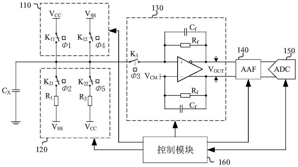
[0051] In the following technical solutions provided by the embodiments of the present application, since the capacitance detection circuit includes: a control module, a driving module, an offsetting module, and a charge transfer module, the driving module is configured to pass the first charging branch under the control of the control module. The detection capacitor is forwardly charged through the second charging branch, or the detection capacitor is reversely charged through the second charging branch; the offsetting module is used to charge the detection capacitor through the first offsetting branch under the control of the control module. The detection capacitor performs basic capacitance cancellation processing, or, under the control of the control module, performs the basic capacitance cancellation processing on the detection capacitor through the second cancellation branch; the charge transfer module is used for The charge of the detection capacitor is transferred to generate an output voltage; the output voltage can be used to determine the capacitance change before and after the detection capacitor is affected by the applied electric field. When applied to self-capacitance detection, it can be eliminated or reduced by charge cancellation. The small detected basic capacitance of the detection capacitor increases the rate of change of the capacitance under the condition that the amount of capacitance change remains unchanged, improves the sensitivity of self-capacitance detection, and finally improves the accuracy of self-capacitance detection.
[0052] The specific implementation of the embodiments of the present application is further described below with reference to the accompanying drawings of the embodiments of the present application.
[0053] In the following embodiments 1 and 2, the self-capacitance detection of one detection capacitor is taken as an example for description. Therefore, in the following embodiments, correspondingly, the number of the driving module and the canceling module is one each. In fact, by extension, from the technical point of view, if there are multiple detection capacitors, multiple drive modules and cancellation modules can be configured correspondingly, or, for a detection capacitor, a drive module and a cancellation module can be configured. module.
[0054] Optionally, when implemented, the driving module may include at least one switch and correspondingly configured voltage sources for forming the first charging branch and the second charging branch, and the offsetting module may include at least one switch and correspondingly forming a voltage source. The voltage source configured by the first cancellation branch and the second cancellation branch, however, it should be noted that the implementation of the driving module and the cancellation module by configuring the switch and the voltage source is only an example, and those of ordinary skill in the art can also Any other drive module that can realize the formation of the first charging branch and the second charging branch, and any other canceling module that can realize the formation of the first offsetting circuit branch and the second offsetting branch can be used.
[0055] Optionally, during implementation, the driving module may include at least two switch units, and the at least two switch units switch switch states under the control of the control module to form the first charging branch or the The second charging branch, thereby eliminating low-frequency noise in the circuit and improving the signal-to-noise ratio. In the following embodiments, the driving module includes two switch units as an example for description.
[0056] Optionally, in implementation, the switch unit is specifically a single-pole single-throw switch unit, and the control module is further configured to control one of the single-pole single-throw switch units to form the first charging branch when one of the single-pole single-throw switch units is closed, or , the second charging branch is formed when another single-pole single-throw switch unit is controlled to be closed.
[0057] Optionally, during implementation, when the detection capacitor is forwardly charged through the first charging branch, the detection capacitor is connected to the forward voltage source through the first charging branch; When the detection capacitor is reversely charged, the detection capacitor is electrically connected to a negative voltage source through the second charging branch.
[0058] Optionally, during implementation, the cancellation module may include at least two switch units, and the at least two switch units switch switch states under the control of the control module to form the first cancellation branch or the The second offset branch. In the following embodiments, the driving module includes two switch units as an example for description.
[0059] Optionally, during implementation, the switch unit is a single-pole single-throw switch unit, and the control module is further configured to control one of the single-pole single-throw switch units to form the first offset branch when one of the single-pole single-throw switch units is closed, or, The second offsetting branch is formed when the other single-pole single-throw switch unit is controlled to be closed.
[0060] Optionally, during implementation, when the basic capacitance cancellation process is performed on the detection capacitor through the first cancellation branch, the cancellation module is connected to the negative voltage source through one end of the first cancellation branch; When the second cancellation branch performs basic capacitance cancellation processing on the detection capacitor, the cancellation module is connected to the forward voltage source through one end of the second cancellation branch.
[0061] Optionally, during implementation, the cancellation module includes a first cancellation resistor and a second cancellation resistor, and when the cancellation module performs cancellation processing on the basic capacitance of the detection capacitor through the first cancellation branch, the detection The capacitor is in the first discharge state through the first cancellation resistor; when the cancellation module cancels the basic capacitance of the detection capacitor through the second cancellation branch, the detection capacitor is in the second discharge state through the second cancellation resistor .
[0062] Optionally, the resistance value of the first cancellation resistor and the resistance value of the second cancellation resistor are not equal.
[0063] Optionally, in the implementation, after the detection capacitor is positively charged by the first charging branch, the basic capacitance cancellation process is performed on the detection capacitor by the first cancellation branch; or, the second charging branch is used to cancel the basic capacitance. After the detection capacitor is reversely charged, the basic capacitance cancellation process is performed on the detection capacitor through two cancellation branches.
[0064] Optionally, during implementation, the charge transfer module includes a differential amplifier circuit, an inverting terminal of the differential amplifier circuit is electrically connected with a common-mode voltage, and a non-inverting terminal of the differential amplifier circuit is performing the detection on the detection capacitor. The non-inverting terminal of the differential amplifying circuit is electrically disconnected from the detection capacitor when charging and canceling the detection capacitor.
[0065] Specifically to the following first and second embodiments, the two switch units specifically included in the driving module 110 are respectively denoted as K 11 , K 12 , the positive voltage source is recorded as Vcc, the negative voltage source is recorded as Vss, the switch unit K 11 , switch unit K 12 All are single-pole single-throw switch units. The two switch units specifically included in the cancellation module 120 are respectively denoted as K 21 , K 22 , The positive voltage source is recorded as Vcc, and the negative voltage source is recorded as Vss. The cancellation module 120 also includes two cancellation resistors, which are respectively denoted as R 1 , R 2. In addition, the transfer module is denoted as 130, which includes a differential amplifier, a feedback resistor Rf, and a feedback capacitor Cf, so as to convert the charge on the detection capacitor into a voltage signal. The output voltage of the transfer module 130 is filtered by an anti-alias filter (AAF) 140, and then sent to an analog-digital converter (ADC) 150 for sampling, and then passed through a digital signal processor. (DIGITAL SIGNAL PROCESSOR, referred to as DSP) performs quadrature (IQ) demodulation, and the obtained raw data is sent to the CPU for coordinate calculation to obtain the touch position. In addition, the control module is marked as 160, which controls the switch unit K 11 , switch unit K12 , switch unit K 21 , switch unit K 22 , switch unit K 3 The control signals are respectively recorded as Φ1, Φ4, Φ2, Φ5, Φ3.
[0066] Figure 1A This is a schematic structural diagram of the capacitance detection circuit in the first embodiment of the present application; Figure 1B This is a schematic diagram of the working sequence of the capacitance detection circuit in the first embodiment of the present application. It should be noted here that, Figure 1B In , when there is an external electric field, the capacitance of the detection capacitor changes, and at the same time, perfect cancellation is achieved, the output voltage of the charge transfer module is Vout.
[0067] Period t1: Specifically, at Figure 1A , when the detection capacitor is positively charged through the first charging branch, the detection capacitor is connected to the forward voltage source Vcc through the first charging branch; the first charging branch is specifically: the control module generates Control signal Φ1 to control switch unit K 11 Closed, so that the detection capacitor Cx is connected to the forward voltage source Vcc, thereby forming a first charging branch for the forward voltage source Vcc to charge the detection capacitor Cx, and the voltage reaches Vcc after the charging is completed. In addition, in the period of t1, except for the switching unit K 11 The other switch units are disconnected under the control of their respective control signals.
[0068] t2 period: after the charging of the detection capacitor is completed through the first charging branch, the switching unit K 11 open, switch unit K 21 Under the control of its control signal Φ2, it is closed to form the first cancellation branch, and the detection capacitor passes through the resistor R 1 (ie, the first cancellation resistor) discharges the voltage source Vss forward (ie, the first discharge state) to cancel the basic capacitance of the detection capacitor. After the discharge is completed, the voltage of the detection capacitor to the system ground In addition, in the period of t2, except for the switching unit K 21 The other switch units are disconnected under the control of their respective control signals.
[0069] Depend on Figure 1A It can be seen that when the basic capacitance cancellation process is performed on the detection capacitor through the first cancellation branch, the cancellation module is connected to the negative voltage source Vss through one end of the first cancellation branch.
[0070] Optionally, in this embodiment, when the cancellation module performs cancellation processing on the basic capacitance of the detection capacitor through the first cancellation branch, the detection capacitor is in a first discharge state through the first cancellation resistor.
[0071] t3 period: after completing the offset processing of the basic capacitance of the detection capacitor through the first offset branch, the switch unit K 3 It is closed under the control of its control signal Φ3. In addition, other switch units are turned off, and the detection capacitor transfers the charge to the charge transfer module, so that the charge transfer module generates the output voltage Vout, and detects the amount of charge transferred from the capacitor Cx to the charge transfer module. is [u(t2)-Vcm]*Cx.
[0072] t4 period: After completing the above-mentioned charge transfer processing in the t3 period, the switching unit K 11 , switch unit K 21 , switch unit K 22 Disconnected under the control of the respective control signal, but the switch unit K 12 It is closed under the control of its control signal Φ4. Due to switching unit K 12 closed to form a second charging branch to charge the detection capacitor, so that the detection capacitor is reversely charged to Vss.
[0073] Time period t5: After completing the charging of the detection capacitor through the second charging branch, the switching unit K 11 , switch unit K 21 , switch unit K 12 Disconnected under the control of the respective control signal, but the switch unit K 22 It is closed under the control of its control signal Φ5, so that the second cancellation branch is formed, and the detection capacitor passes through the resistor R 2 (ie, the second offset resistor) discharges the voltage source Vcc in the reverse direction (ie, the second discharge state), and after the discharge is completed, the voltage of the detection capacitor to the system ground
[0074] t6 period: after completing the offset processing of the basic capacitance of the detection capacitor through the second offset branch, the switching unit K 3 It is closed under the control of its control signal Φ5, other switch units are opened under the control of their respective control signals, the detection capacitor transfers the charge to the charge transfer module, so that the charge transfer module generates the output voltage Vout, and the detection capacitor Cx transfers the charge to the charge transfer module. The amount of charge is [u(t5)-Vcm]*Cx.
[0075] Optionally, in this embodiment, the resistance value of the first cancellation resistor is set not to be equal to the resistance value of the second cancellation resistor. Since the charging and discharging speeds of the circuits are not the same, by setting the size of the first offset resistor not equal to the size of the second offset resistor, when there is no touch operation, the voltage on the detection capacitor is exactly Vcm, so as to achieve perfect offset, to improve the sensitivity of touch detection.
[0076] The above t1 and t4 are charging stages, t2 and t5 are offset stages, t3 and t6 are charge transfer stages, and t1 to t6 are a detection period T. The process of t4 to t6 is actually the inverse process of t1 to t3, thereby weakening the highly correlated noise, especially the low-frequency noise, in the circuits of these two processes.
[0077] In the above embodiment, the charge transfer module includes a differential amplifier circuit (such as a double-ended differential amplifier), the inverting terminal of the differential amplifier circuit is electrically connected to the common mode voltage Vcm, and the non-inverting terminal of the differential amplifier circuit is in the When performing charge transfer processing on the detection capacitor, it is electrically connected to the detection capacitor, so as to realize the transfer of the charge of the detection capacitor to the charge transfer module, and the non-inverting terminal of the differential amplifier circuit is charging and canceling the detection capacitor. It is electrically disconnected from the detection capacitor during processing.
[0078] Figure 1C This is a schematic flowchart of the capacitance detection method in the first embodiment of the application; for the above Figure 1A In the shown capacitance detection circuit, in one detection cycle, the corresponding capacitance detection method includes:
[0079] The embodiment of the present application provides a capacitance detection method, which includes:
[0080] S101, the drive module positively charges the detection capacitor through the first charging branch under the control of the control module;
[0081] combined with the above Figure 1A , switch unit K 11 It is in a closed state under the control of the control module to form the first charging branch.
[0082] When the detection capacitor is forwardly charged through the first charging branch in step S101, the detection capacitor is connected to the forward voltage source Vcc through the first charging branch.
[0083] S102. The cancellation module performs basic capacitance cancellation processing on the detection capacitor through the first cancellation branch under the control of the control module.
[0084] In step S102, the cancellation module includes at least two switch units, and correspondingly, the control module controls one of the switch units K 21 The first counteracting branch is formed when closed.
[0085] In step S102, when the basic capacitance cancellation process is performed on the detection capacitor through the first cancellation branch, the cancellation module is connected to the negative voltage source Vss through one end of the first cancellation branch.
[0086] S103, the charge transfer module performs transfer processing on the charge of the detection capacitor to generate an output voltage;
[0087] like Figure 1A shown, the switch unit K 3 When closed, other switch units are in an open state, and the charge on the detection capacitor is transferred to the charge transfer module to generate the output voltage Vout.
[0088] S104, the drive module reversely charges the detection capacitor through the second charging branch under the control of the control module;
[0089] combined with the above Figure 1A , switch unit K 12 It is in a closed state under the control of the control module to form the second charging branch.
[0090] combined with the above Figure 1A , when the detection capacitor is reversely charged through the second charging branch, the detection capacitor is electrically connected to the negative voltage source Vss through the second charging branch.
[0091] S105, the cancellation module performs the cancellation process of the basic capacitance on the detection capacitor through the second cancellation branch under the control of the control module;
[0092] In this embodiment, in step S105, the cancellation module includes at least two switch units, and correspondingly, the control module controls one of the switch units K 22 The second counteracting branch is formed when closed.
[0093] In this embodiment, in step S105, when the basic capacitance cancellation process is performed on the detection capacitor through the second cancellation branch, the cancellation module is connected to the forward voltage source Vcc through one end of the second cancellation branch .
[0094] S106, the charge transfer module performs transfer processing on the charge of the detection capacitor to generate an output voltage.
[0095] like Figure 1A shown, the switch unit K 3 When closed, other switch units are in an open state, and the charge on the detection capacitor is transferred to the charge transfer module.
[0096] In order to effectively detect the capacitance change of the detection capacitor, several detection cycles may be set, and the above steps S101-S105 may be performed in each detection cycle.
[0097] The most ideal situation is that when there is no touch operation, at the end of t2 and t5, the voltage on the detection capacitor Cx is exactly Vcm, that is, when u(t2)=u(t5)=Vcm, the amount of charge transferred is 0. , so as to achieve perfect cancellation. Then when there is no touch, the output voltage of the charge transfer module is 0. When there is a touch operation, the output voltage of the charge transfer module is not 0. At this time, the output voltage of the amplifier is completely generated by the touch, and a larger magnification can be used to increase the amplitude of the output voltage to facilitate detection, thereby improving the touch sensitivity.
[0098] In perfect cancellation, the relationship is satisfied:
[0099]
[0100]
[0101] available and
[0102] Optionally, in this embodiment, the size of R1 is set to be unequal to the size of R2. Since the charging and discharging speeds of the circuits are different, the size of R1 is set not equal to the size of R2, so that when there is no touch operation, the detection The voltage across the capacitor is exactly Vcm, allowing perfect cancellation to improve the sensitivity of touch detection.
[0103]Considering that t1-t3 and t4-t6 are symmetrical processes, t1 and t4, t3 and t6 will be set to be the same, so it is expected that the values of t2 and t5 are also the same, or close to each other. According to the operating frequency of the circuit, first determine the target values of t2 and t5, and then determine the calculated values of resistors R1 and R2 according to the values of Vcc, Vss, Vcm and the estimated value of Cx. Due to the limited offset resistance range of the actual chip, the set values of R1 and R2 will deviate from the calculated values. The set values of R1 and R2 can only approximate the calculated values as much as possible. Therefore, when determining the settings of R1 and R2 After the value is adjusted, fine-tune the lengths of t2 and t5, so that the actual values of t2 and t5 are equal or as close as possible, so that the positive and negative processes can reach or approach a state of perfect cancellation. Then the gain of the amplifier circuit can be increased to improve the sensitivity of touch detection.
[0104] Figure 2A This is a schematic structural diagram of the capacitance detection circuit in the second embodiment of the present application; Figure 2B This is a schematic diagram of the working sequence of the capacitance detection circuit in the second embodiment of the present application. The structure of the driving module is the same as the above-mentioned embodiment in that one of the switch units K 11 It is a single-pole single-throw switch unit, and another switch unit K 12 It is a single-pole double-throw switch unit to realize the formation of a first charging branch or a second charging branch. In addition, in the structure of the cancellation module, in the above-mentioned switch unit K 21 and K 22 On the basis of adding the switch unit K 23 , the switch unit K 23 For SPDT switch unit, with switch unit K 21 and K 22 The cooperation is realized to form the first cancellation branch or the second cancellation branch. In this embodiment, the switch unit K 11 , switch unit K 12 , switch unit K 21 , switch unit K 22 , switch unit K 23 , switch unit K 4 The control signals are respectively control signals Φ1, Φ5, Φ2, Φ3, Φ5, Φ4. Here, it should be noted that although the reference numerals of the control signals are the same as those in the first embodiment, it does not mean that the control signals are essentially the same as the control signals in the first embodiment.
[0105] The timing of the control is different from the implementation:
[0106] In phase t1, the switch unit K 11 Closed under the control of the control signal Φ1, the switch unit K 12 Under the control of the control signal Φ5, the contact 1 is contacted to form the first charging branch, the switch unit K 23 Contact 1 is touched under control signal Φ5, but due to switch unit K 21 It is disconnected under the control of the control signal Φ2, and the offset module does not work.
[0107] During the period of t2, the switch unit K 11 Turned off under the control of the control signal Φ1, the switch unit K 21 The switch unit K is closed under the control of the control signal Φ2 22 It is disconnected under the control of the control signal Φ3, thereby forming the first cancellation branch, and after the end of the t2 period, the voltage of the detection capacitor is u(t2);
[0108] During the period of t3, the switch unit K 3 Closed under the control of the control signal Φ4, the switch unit K 11 , K 21 , K 21 It is turned off under the control of the respective control signals, and the charge on the detection capacitor is transferred to the charge transfer processing module, and the amount of the transferred charge is [u(t2)-Vcm]*Cx.
[0109] In the stage t4, the switch unit K 11 Closed under the control of the control signal Φ1, the switch unit K 12 Under the control of the control signal Φ5, the contact 2 is contacted to form the second charging branch, the switch unit K 23 Contact 2 is touched under control signal Φ5, but due to switch unit K 21 It is disconnected under the control of the control signal Φ2, and the offset module does not work.
[0110] During the period of t5, the switch unit K 11 Turned off under the control of the control signal Φ1, the switch unit K 23 Contact 2 under the control of control signal Φ5, switch unit K 22 The switch unit K is closed under the control of the control signal Φ3 21 It is disconnected under the control of the control signal Φ2, thereby forming the second cancellation branch. After the period of t5 ends, the voltage of the detection capacitor is u(t5);
[0111] During the period of t6, the switch unit K 3 Closed under the control of the control signal Φ4, the switch unit K 11 , K 21 , K 21 It is turned off under the control of the respective control signals, and the charge on the detection capacitor is transferred to the charge transfer processing module, and the amount of the transferred charge is [u(t5)-Vcm]*Cx.
[0112] Optionally, in this embodiment, the size of R1 is set not equal to the size of R2. Since the charging and discharging speeds of the circuits are different, the size of R1 is set not equal to the size of R2, so that when there is no touch operation, the detection capacitor can be detected. The voltage on is exactly Vcm, which enables perfect cancellation to improve the sensitivity of touch detection.
[0113] see Figure 2A It can be seen from the above process that the above t1 and t4 are charging stages, t2 and t5 are offset stages, t3 and t6 are charge transfer stages, and t1 to t6 are a detection period T. The process of t4 to t6 is actually the inverse process of t1 to t3, thereby weakening the highly correlated noise, especially the low-frequency noise, in the circuits of these two processes. The most ideal situation is that when there is no touch operation, at the end of t2 and t5, the voltage on the detection capacitor Cx is exactly Vcm, that is, when u(t2)=u(t5)=Vcm, the amount of charge transferred is 0. , so as to achieve perfect cancellation. Then when there is no touch, the output voltage of the charge transfer module is 0. When there is a touch operation, the output voltage of the charge transfer module is not 0. At this time, the output voltage of the amplifier is completely generated by the touch, and a larger magnification can be used to increase the amplitude of the output voltage to facilitate detection, thereby improving the touch sensitivity.
[0114] In perfect cancellation, the relationship is satisfied:
[0115]
[0116]
[0117] available and
[0118] Considering that t1-t3 and t4-t6 are symmetrical processes, t1 and t4, t3 and t6 will be set to be the same, so it is expected that the values of t2 and t5 are also the same, or close to each other. According to the operating frequency of the circuit, first determine the target values of t2 and t5, and then determine the calculated values of resistors R1 and R2 according to the values of Vcc, Vss, Vcm and the estimated value of Cx. However, due to the limited offset resistance range of the actual chip, the set values of R1 and R2 will deviate from the calculated values. In fact, it is only possible to approximate the calculated values as much as possible. After determining the actual values of R1 and R2, fine-tune the time lengths of t2 and t5, so that the actual values of t2 and t5 are equal or as close as possible, so that both the positive and negative processes reach or are close to reaching a state of perfect cancellation. Then the gain of the amplifier circuit can be increased to improve the sensitivity of touch detection.
[0119] Figure 2A The shown capacitance detection circuit implements capacitance detection in a similar way as described above Figure 1A Example shown.
[0120] Further, in terms of product realization, it actually includes several detection capacitors, and then each of the detection capacitors can be configured with a drive module, a cancellation module, and a charge transfer module. At the same time, when the charge transfer module includes a differential amplifier circuit, the differential principle can be used to realize the similar characteristics between adjacent detection channels when detecting the capacitance change of the detection capacitor, so as to achieve noise suppression and ultimately improve the signal-to-noise ratio. . The following description will be given by taking the processing of two detection capacitors (respectively denoted as Cx1 and Cx2 ) as an example.
[0121] Figure 3A This is a schematic structural diagram of a capacitance detection circuit in Embodiment 3 of the present application; Figure 3B A schematic diagram of the time sequence of capacitance detection in the third embodiment of the present application; as Figure 3A As shown, a drive module 110 and a cancellation module 120 are respectively set for the detection capacitors Cx1 and Cx2. The difference from the above embodiment is that in the charge transfer processing stage, the detection capacitors Cx1 and Cx2 are respectively connected with the differential amplifier in the charge transfer processing 130. connected, in effect there is a charge transfer to the charge transfer processing module at the same time. exist Figure 3A Among them, the cancellation resistances in one of the cancellation modules 120 are R1 and R2, and the cancellation resistances in the other cancellation module 120 are R3 and R4.
[0122] Therefore, in each time period from t1 to t6, the switches in the driving module and the cancellation module corresponding to the detection capacitors Cx1 and Cx2 are turned on or off at the same time.
[0123] At the end of time t2, the voltage of the detection capacitor Cx1 to the system ground
[0124] At the end of time t2, the voltage of the detection capacitor Cx2 to the system ground
[0125] At time t3, the amount of charge transferred from the detection capacitor Cx1 to the charge transfer processing module is ΔQ 1 =[u 1 (t 2 )-V CM ]C X1 , the amount of charge transferred from the detection capacitor Cx2 to the charge transfer processing module is ΔQ 2 =[u 2 (t 2 )-V CM ]C X2 , according to the size of ΔQ1 and ΔQ2, there are the following situations:
[0126] If ΔQ1>ΔQ2, the output Vout of the amplifier circuit is a negative voltage;
[0127] If ΔQ1=ΔQ2, the output Vout of the amplifier circuit is 0;
[0128] If ΔQ1
[0129] Similarly, at time t5, the above-mentioned relationship exists between the amount of charge transferred from the detection capacitor Cx1 to the charge transfer processing module and the amount of charge transferred from the detection capacitor Cx2 to the charge transfer processing module. In circuit design, from a theoretical point of view, in order to achieve perfect cancellation, ΔQ1=ΔQ2 should be realized.
[0130] In this embodiment, two adjacent detection capacitors are charged, cancelled and transferred at the same time, and the amplified signal is output to the subsequent stage circuit through the differential amplifier. In a touch control system, adjacent detection channels often have similar basic capacitances, similar temperature drifts with temperature changes, and similar noise characteristics. Therefore, this embodiment can suppress noise, improve the signal-to-noise ratio, and have the ability to suppress temperature drift. Further, when an electric field is applied due to a touch, it can be determined by the direction of Vout in the third embodiment above that the capacitance change of the one of the two detection capacitors is relatively large, and then according to the relative magnitude relationship of the capacitances, Thereby, the position of the touch is further determined.
[0131] Figure 4is an exemplary structural diagram of the control circuit in the fourth embodiment of the present application; as Figure 4 As shown, it includes several counters (for example, if there are five, they are respectively denoted as counter1, counter2, counter3, counter4, and counter5), and the output of each counter controls the switch unit in the above-mentioned first or second embodiment, that is, the formation of The above control signals Φ1-Φ5. These counters share the same clock signal sys-clk to obtain the same clock accuracy. The higher the clock frequency, the higher the precision of time control that can be obtained. Therefore, the clock signal generally uses the main clock of the touch detection system, and its main frequency is the highest in the entire system. Each counter also has its own data line connected to the corresponding register. By modifying the value of the register, the counting period and action time of these counters are modified, so as to achieve the effect of controlling the working sequence of the switch.
[0132] Figure 5 is an exemplary structural diagram of the offset resistance in the fifth embodiment of the present application; as Figure 5 As shown, it mainly includes a plurality of resistors (Res1...Resn) and a plurality of switches (SW1...SWn). Each resistor is connected in parallel with a switch to form a combination, and several such combinations are connected in series. Each switch has a control wire, and the control wires of all switches are connected together to the register. By modifying the value Code[n:0] of the register, different switches can be turned on and off, thereby controlling the resistance value of the cancellation resistor.
[0133] In the above-mentioned embodiment, considering that the discharge rates of the two cancellation branches will be different, it is impossible to achieve perfect cancellation of the basic capacitance of the detection capacitor (or called as complete cancellation as possible), and each cancellation branch is set separately A cancellation resistor is designed, so that the discharge rates of the two cancellation branches are as equal as possible by designing the size of the cancellation resistance in each cancellation branch, thereby ensuring the realization of perfect cancellation. Therefore, in the circuit design of the cancellation module, referring to FIG. 1 , one end of the first cancellation resistor in the first cancellation branch is directly connected to the voltage source Vss, and the other end is connected to the switch unit K 21 Similarly, one end of the second canceling resistor in the second canceling branch is directly connected to the voltage source Vcc, and the other end is connected to the switch unit K 22 connected so that the two cancelling circuits are independent of each other. In addition, in the circuit design of the cancellation module, the first cancellation resistor in the first cancellation branch is set in the switch unit K 21 and K 23 between, the first offset resistance can pass through the switch unit K 21 Connected with the voltage source Vss; the second offset resistor in the second offset branch is set in the switch unit K 22 and K 23 between, the second offset resistor can pass through the switch unit K 22 Connected to the voltage source Vcc; and through the switch unit K 23 The contacts 1 and 2 are switched, thereby forming a first cancelling branch and a second cancelling branch, respectively.
[0134] In addition, each voltage source used in the above embodiments can be generated by a voltage source generating module according to requirements.
[0135] The embodiment of the present application further provides an electronic device, which includes the touch control chip described in any one of the embodiments of the present application.
[0136] For this reason, in a specific application scenario, the larger the basic capacitance of the detection capacitor, the smaller the resistance of the offset resistor, and vice versa, the greater the offset resistor. In addition, due to the use of a negative voltage source, the detectable output voltage is increased, thereby improving the signal-to-noise ratio.
[0137] It should be noted that in the above embodiments, although a single switch unit is used as an example for description, in fact, it can also be implemented in the form of a circuit combination structure, wherein the components can be any electronic device with an on-off function. The components only need to be able to form a charging branch and an offsetting branch, and can realize the switching from the charging branch to the offsetting branch, and make the detection circuit enter the charge transfer state.
[0138] In addition, when the touch detection is implemented based on mutual capacitance detection, if the basic capacitance of the mutual capacitance is relatively large so as to affect the change rate of the mutual capacitance, the ideas of the following embodiments of the present application can also be applied.
[0139] The electronic devices of the embodiments of the present application exist in various forms, including but not limited to:
[0140] (1) Mobile communication equipment: This type of equipment is characterized by having mobile communication functions, and its main goal is to provide voice and data communication. Such terminals include: smart phones (eg iPhone), multimedia phones, feature phones, and low-end phones.
[0141] (2) Ultra-mobile personal computer equipment: This type of equipment belongs to the category of personal computers, has computing and processing functions, and generally has the characteristics of mobile Internet access. Such terminals include: PDAs, MIDs, and UMPC devices, such as iPads.
[0142] (3) Portable entertainment equipment: This type of equipment can display and play multimedia content. Such devices include: audio and video players (eg iPod), handheld game consoles, e-books, as well as smart toys and portable car navigation devices.
[0143] (4) Server: A device that provides computing services. The composition of the server includes a processor, a hard disk, a memory, a system bus, etc. The server is similar to a general computer architecture, but due to the need to provide highly reliable services, the processing power, stability , reliability, security, scalability, manageability and other aspects of high requirements.
[0144] (5) Other electronic devices with data interaction function.
[0145] So far, specific embodiments of the present subject matter have been described. Other embodiments are within the scope of the appended claims. In some cases, the actions recited in the claims can be performed in a different order and still achieve desirable results. Additionally, the processes depicted in the figures do not necessarily require the particular order shown, or sequential order, to achieve desirable results. In certain embodiments, multitasking and parallel processing may be advantageous.
[0146] It should also be noted that the terms "comprising", "comprising" or any other variation thereof are intended to encompass a non-exclusive inclusion such that a process, method, article or device comprising a series of elements includes not only those elements, but also Other elements not expressly listed, or which are inherent to such a process, method, article of manufacture, or apparatus are also included. Without further limitation, an element qualified by the phrase "comprising a..." does not preclude the presence of additional identical elements in the process, method, article of manufacture, or device that includes the element.
[0147] Each embodiment in this specification is described in a progressive manner, and the same and similar parts between the various embodiments may be referred to each other, and each embodiment focuses on the differences from other embodiments. In particular, as for the system embodiments, since they are basically similar to the method embodiments, the description is relatively simple, and for related parts, please refer to the partial descriptions of the method embodiments.
[0148] The above descriptions are merely examples of the present application, and are not intended to limit the present application. Various modifications and variations of this application are possible for those skilled in the art. Any modification, equivalent replacement, improvement, etc. made within the spirit and principle of this application shall be included within the scope of the claims of this application.
PUM


Description & Claims & Application Information
We can also present the details of the Description, Claims and Application information to help users get a comprehensive understanding of the technical details of the patent, such as background art, summary of invention, brief description of drawings, description of embodiments, and other original content. On the other hand, users can also determine the specific scope of protection of the technology through the list of claims; as well as understand the changes in the life cycle of the technology with the presentation of the patent timeline. Login to view more.
Similar technology patents
Acceleration sensor and manufacturing method thereof
Owner:LAPIS SEMICON CO LTD
Three-dimensional carbon nano-material field effect flexible force sensing element and preparation method
Owner:SOUTHEAST UNIV
CircRNA markers for early diagnosis of lung adenocarcinoma and application thereof
Owner:SOUTHEAST UNIV
Power distribution network failure data self-synchronizing method based on instantaneous amplitude change
Owner:STATE GRID CORP OF CHINA +1
Preparation method and application of sinonovacula constricta enzymolysis polypeptide
Owner:ZHEJIANG OCEAN UNIV
Classification and recommendation of technical efficacy words
- high sensitivity
System and method for optical coherence imaging
Owner:THE GENERAL HOSPITAL CORP
Three-axis integrated MEMS accelerometer
Owner:VAGANOV VLADIMIR +1
Capacitive micromachined acoustic transducer
Owner:NEOMEMS TECH INC WUXI CHINA
Patterning process, resist composition, and acetal compound
Owner:SHIN ETSU CHEM CO LTD