

Method of creating wafer shape data
Patent Information
- Authority / Receiving Office
- CN · China
- Patent Type
- Applications(China)
- Current Assignee / Owner
- SHIN-ETSU HANDOTAI CO LTD
- Publication Date
- 2021-04-09
Smart Images
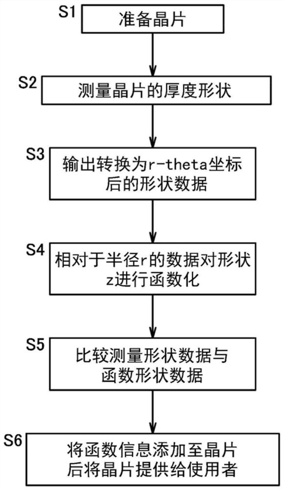
Figure 1 
Figure 2 
Figure 3
Abstract
Description
technical field
[0001] The invention relates to a method for converting the shape of a wafer into data through a function. Background technique
[0002] When wafers such as silicon wafers are shipped to users, SFQR (Site Frontside ref.least sQuare Range), SBIR (Site Backside ref.IdealRange), ESFQR (Edge Site Frontside ref.least sQuare Range) and other flatness parameters. Although these parameters are sufficient to be used as a certain standard for classifying the flatness of wafers, they are substitute parameters that cannot visualize the shape of a wafer. Therefore, it is necessary to pre-measure the shape of the wafer on the platform in the pre-processing before burning the device pattern to the wafer in the stepping procedure.
[0003] Here, there are the following Patent Documents 1 to 3 regarding the measurement of the wafer shape. Patent Document 1 describes a method of measuring the cross-sectional shape of a workpiece such as a silicon wafer. Specifically, Paten...