Supercharge Your Innovation With Domain-Expert AI Agents!

Printed circuit board micro defect detection method based on ACYOLOV4_CSP

A printed circuit board and defect detection technology, which is applied in neural learning methods, image data processing, image enhancement, etc., can solve the problems of accuracy degradation and achieve high-precision detection, low cost, and strong robustness

Pending Publication Date: 2021-04-13
XIAMEN UNIV TAN KAH KEE COLLEGE
View PDF5 Cites 7 Cited by
  • Summary
  • Abstract
  • Description
  • Claims
  • Application Information

AI Technical Summary

Problems solved by technology

The existing method is based on other lightweight networks, such as the detection method based on MoblieNet, which optimizes the speed of TTD-net, but there is a significant drop in accuracy

Method used


Image

  • Printed circuit board micro defect detection method based on ACYOLOV4_CSP
  • Printed circuit board micro defect detection method based on ACYOLOV4_CSP
  • Printed circuit board micro defect detection method based on ACYOLOV4_CSP

Examples


Embodiment

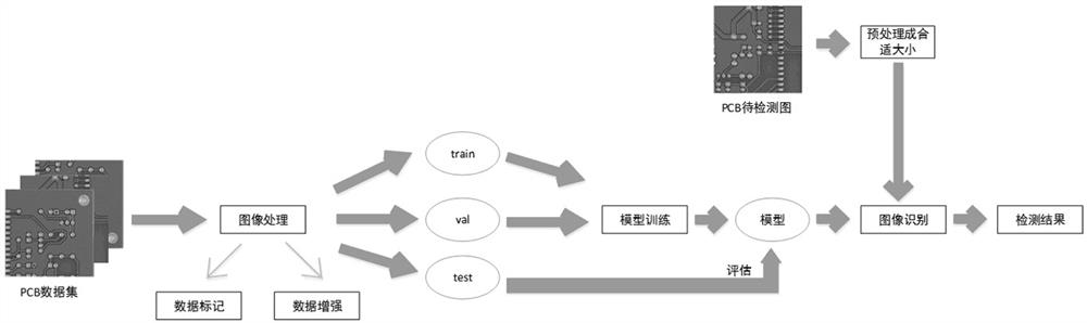
[0055] The operating system of the computer used by the inventive method is Ubuntu16.04, and the graphics card is NVIDIA RTX 20808G. The original dataset used by this method is the PCB defect open dataset (http: / / robotics.pkusz.edu.cn / resources / dataset / ). For the convenience of evaluating performance, the data set generated by cropping, flipping and other operations is consistent with the data set shared in this link (https: / / pan.baidu.com / s / 1eAxDF4txpgMInxbmNDX0Zw). Method execution is mainly divided into the following steps:

[0056] 1. Data set analysis and preparation

[0057] The original data set contains 693 images, covering 6 common types of tiny defects of printed circuit boards: missing drill hole (missing_hole), mouse bite (mouse_bite), open circuit (open_circuit), short circuit (short), uneven line (spur) , Miscellaneous copper (spurious_copper). Common 6 types of defects such as Figure 4 (a) - Figure (f) shown.

[0058] The data set generated by cropping, fl...


PUM


Abstract

The invention relates to a printed circuit board micro defect detection method based on ACYOLOV4_CSP. The method comprises the following steps: S1, labeling each picture of a high-resolution original data set by using a LabelImg labeling tool, namely labeling the defect category and position of the printed circuit board; after labeling is completed, preprocessing the labeled data set to obtain a training set; S2, feeding the training set to an ACYOLOV4-CSP network to obtain an ACYOLOV4CSP model for detecting the micro defects of the printed circuit board; and S3, detecting the image of the printed circuit board to be detected by using the ACYOLOV4CSP model for detecting the tiny defects of the printed circuit board, if the defects exist, outputting an image with a detection frame and category information, and if the defects do not exist, outputting a result image which is the same as the input image. According to the method, the defects of the printed circuit board can be quickly and accurately positioned and classified, and the optimal balance between the speed and the precision is realized.

Description

technical field [0001] The invention relates to the field of machine vision, the field of printed circuit board manufacturing and the field of defect detection of printed circuit boards, in particular to an ACYOLOV4_CSP-based micro defect detection method of printed circuit boards. Background technique [0002] Printed Circuit Board (PCB) is one of the important parts of the electronics industry, which provides support for the fixing, assembly and connection of electronic components. Due to its advantages of high density, assembleability and maintainability, it is Widely used in communication electronic equipment, military weapon systems, computers and other fields. Defect detection of printed circuit boards can detect defects in printed circuit boards in time, avoid affecting subsequent use, and even cause safety problems, providing a guarantee for product quality control. [0003] Existing printed circuit board defect detection is mainly divided into manual detection, tra...

Claims


Application Information

Patent Timeline
Patent Type & Authority Applications(China)
IPC IPC(8): G06T7/00G06N3/04G06N3/08G06K9/62
CPCG06T7/0004G06N3/08G06T2207/30141G06N3/045G06F18/2414G06F18/253G06F18/214
Inventor 郭一晶曾翊昕邱义詹俦军钟林威
Owner XIAMEN UNIV TAN KAH KEE COLLEGE
Features
  • R&D
  • Intellectual Property
  • Life Sciences
  • Materials
  • Tech Scout
  • Unparalleled Data Quality
  • Higher Quality Content
  • 60% Fewer Hallucinations
Learn More