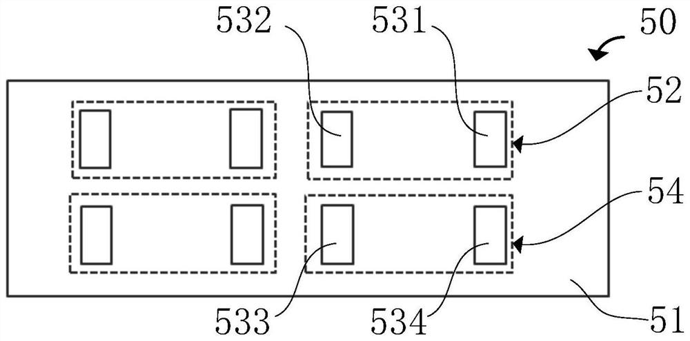
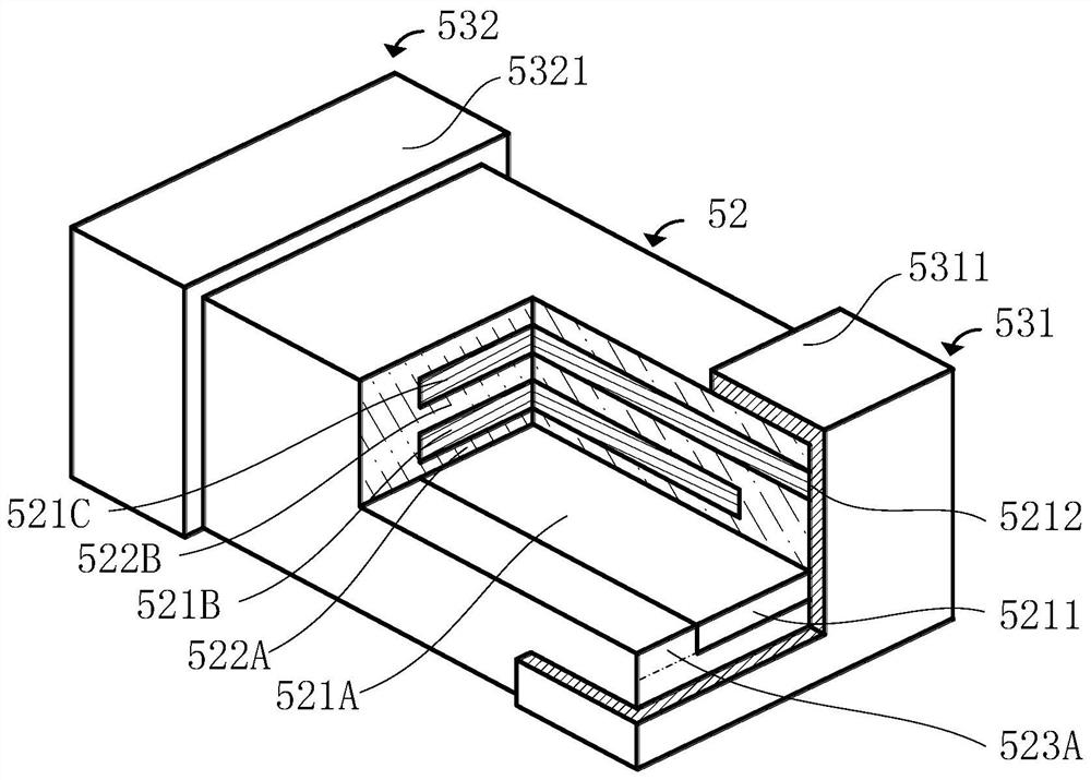
Gasket and manufacturing method thereof, and packaging structure and manufacturing method thereof
A gasket and resistance structure technology, applied in the field of semiconductor devices, can solve problems such as difficulties, occupying a large space, limiting the space of passive components, etc., and achieve good electrical performance, save space, and reduce the effect of devices
- Summary
- Abstract
- Description
- Claims
- Application Information
AI Technical Summary
Problems solved by technology
Method used
Image
Examples
Embodiment Construction
[0071] For a better understanding of the application, various aspects of the application will be described in more detail with reference to the accompanying drawings. It should be understood that these detailed descriptions are descriptions of exemplary embodiments of the application only, and are not intended to limit the scope of the application in any way. Throughout the specification, the same reference numerals refer to the same elements. The expression "and / or" includes any and all combinations of one or more of the associated listed items.
[0072] It should be noted that in this specification, expressions of first, second, third, etc. are only used to distinguish one feature from another, and do not represent any limitation on the features. Accordingly, a first electrode discussed hereinafter may also be referred to as a second electrode without departing from the teachings of the present application. vice versa.
[0073] In the drawings, the thickness, size and sha...
PUM
 Abstract
Description
Claims
Application Information


