Manufacturing method of semiconductor device

A manufacturing method and semiconductor technology, applied in the direction of semiconductor devices, electric solid devices, transistors, etc., can solve problems such as the collapse of insulating layer materials

Active Publication Date: 2021-04-13
CHANGXIN MEMORY TECH INC
View PDF5 Cites 2 Cited by
  • Summary
  • Abstract
  • Description
  • Claims
  • Application Information

AI Technical Summary

Problems solved by technology

[0003] Based on this, it is necessary to provide a method for manufacturing a semiconductor device for the possible collapse of the insulating layer material above the miniaturized bit lines.

Method used


Image

  • Manufacturing method of semiconductor device
  • Manufacturing method of semiconductor device
  • Manufacturing method of semiconductor device

Examples


Embodiment Construction

[0045] In order to make the above objects, features and advantages of the present invention more comprehensible, specific implementations of the present invention will be described in detail below in conjunction with the accompanying drawings. In the following description, numerous specific details are set forth in order to provide a thorough understanding of the present invention. However, the present invention can be implemented in many other ways different from those described here, and those skilled in the art can make similar improvements without departing from the connotation of the present invention, so the present invention is not limited by the specific implementations disclosed below.

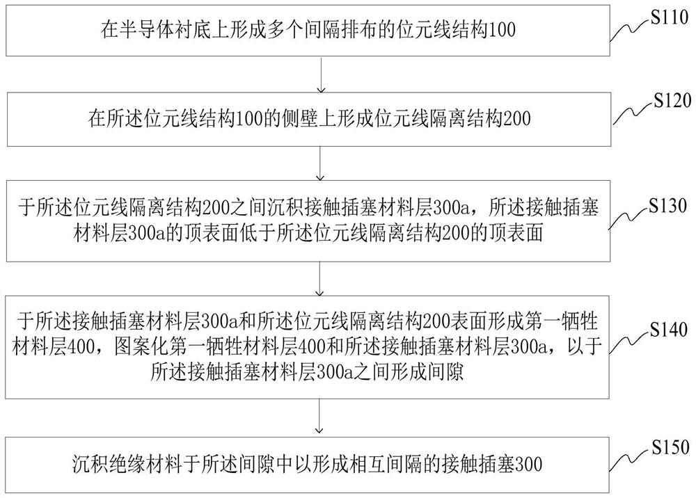
[0046] See figure 1 , an embodiment of the present invention provides a method for manufacturing a semiconductor device, including:

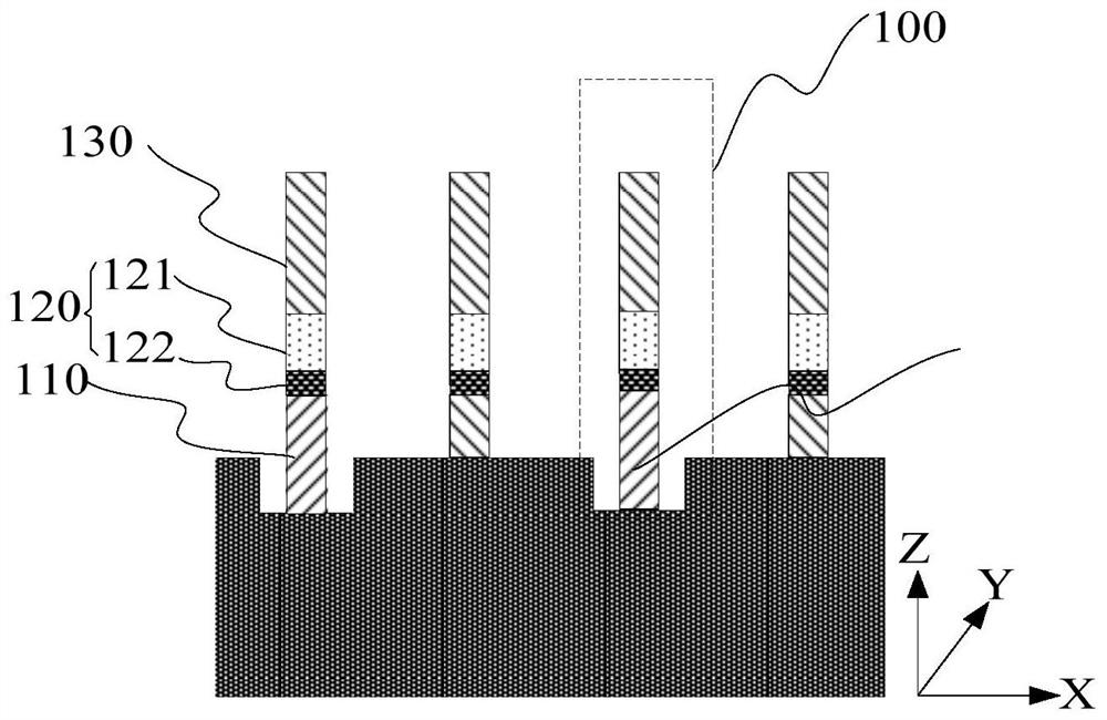
[0047] Step S110, forming a plurality of bit line structures 100 arranged at intervals on the semiconductor substrate;

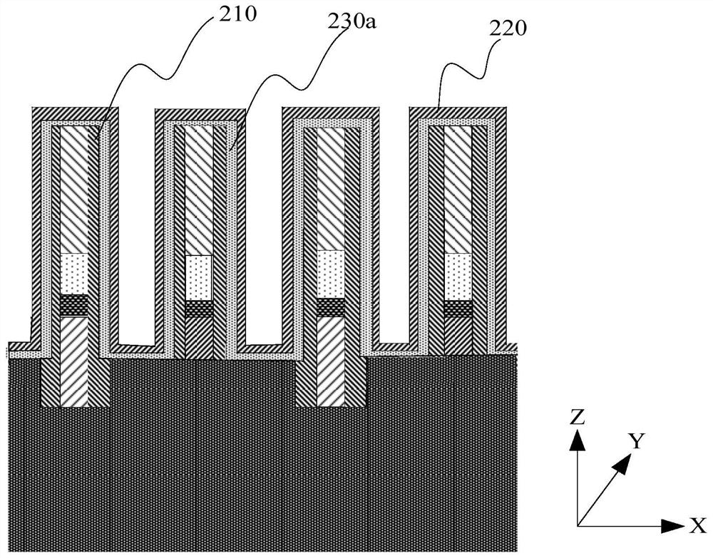
[0048] Step S120, forming a ...


PUM


Abstract

The invention relates to a manufacturing method of a semiconductor device. The manufacturing method comprises the following steps: forming a bit line isolation structure on the side wall of a bit line structure; depositing a contact plug material layer between the bit line isolation structures, wherein the top surface of the contact plug material layer is lower than the top surfaces of the bit line isolation structures; forming a first sacrificial material layer on the surfaces of the contact plug material layer and the bit line isolation structure, patterning the first sacrificial material layer and the contact plug material layer, and forming a gap between the contact plug material layers; and depositing an insulating material in the gap to form contact plugs spaced apart from each other. According to the invention, the consumption of the bit line isolation structure is reduced by utilizing the high etching selection ratio among the contact plug material, the first sacrificial material layer and the bit line isolation structure, so that the thickness of the bit line isolation structure is reduced, and the critical size of the bit line is reduced. And the contact plug material layer is used for providing support for the bit line isolation structure, so that the bit line isolation structure is prevented from collapsing and being separated in the subsequent process.

Description

technical field [0001] The invention relates to the technical field of semiconductor storage devices, in particular to a method for manufacturing a semiconductor device. Background technique [0002] With the development of semiconductor devices, miniaturization of bit lines is an important direction. The reduced critical size of bit lines can allow enough space for capacitor connection lines to improve the performance of semiconductor devices. However, as the critical dimension shrinks, the leakage probability between the bit line and the capacitor contact line increases. Usually, the thickness of the insulating material is increased to improve this phenomenon. The increase in the thickness of the insulating material and the reduction in size will cause the graphics to tilt during the manufacturing process. It even collapses, which affects the product yield and limits the possibility of further reducing the critical dimension of the bit line. Contents of the invention ...

Claims


Application Information

Patent Timeline
Patent Type & Authority Applications(China)
IPC IPC(8): H01L27/108
CPCH10B12/30H10B12/485H10B12/482
Inventor 李昇
Owner CHANGXIN MEMORY TECH INC
Why Eureka
Try Eureka