A pcb buffer design method and pcb board for preventing bga tin cracking
A technology of PCB board and design method, applied in the direction of printed circuit, printed circuit parts, printed circuit stress/deformation reduction, etc., can solve the problems of many tin cracks in BGA chips, influence of BGA chip quality, and low repairability. To achieve the effect of reliable design principle, prominent substantive features and simple structure
- Summary
- Abstract
- Description
- Claims
- Application Information
AI Technical Summary
Problems solved by technology
Method used
Image
Examples
Embodiment 1
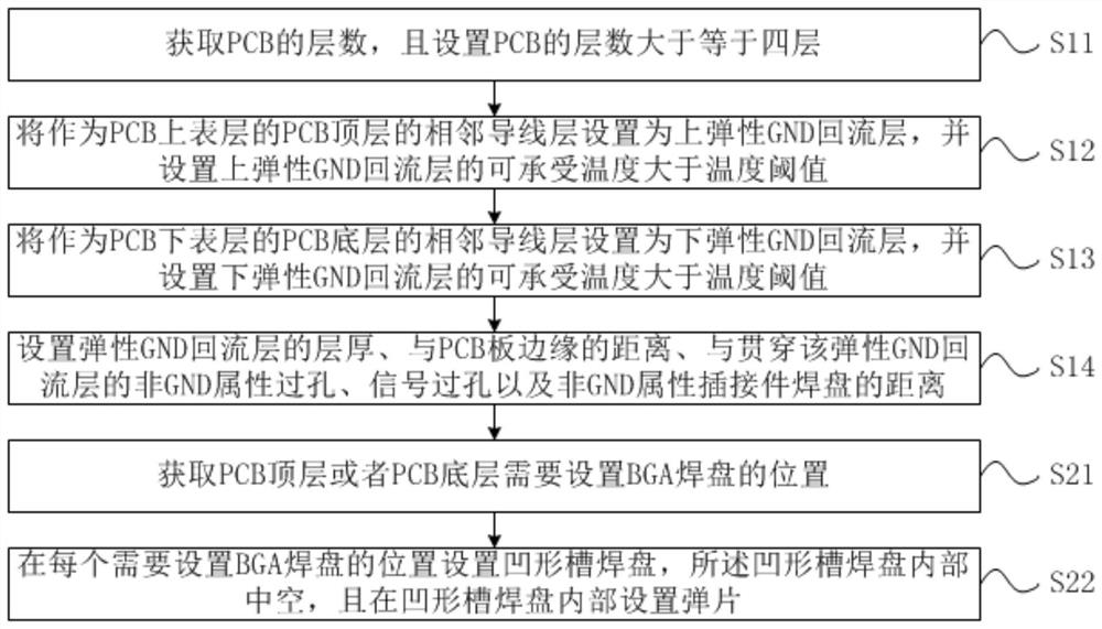
[0060] like figure 1 As shown, the present invention provides a PCB buffer design method for preventing BGA tin cracks, comprising the following steps:
[0061] S1. Obtain the number of layers of the PCB, and set the adjacent layers of the upper surface layer and the adjacent layers of the lower layer of the PCB as elastic GND reflow layers;
[0062] S2. Obtain the position of the BGA pad corresponding to the pin of the BGA chip on the surface of the PCB, set a concave groove inside the BGA pad, and set a shrapnel in the concave groove.
Embodiment 2
[0064] like figure 2 As shown, the present invention provides a PCB buffer design method for preventing BGA tin cracks, which is characterized in that it includes the following steps:
[0065] S1. Obtain the number of layers of the PCB, and set the adjacent layer of the upper surface layer and the adjacent layer of the lower layer of the PCB as the elastic GND reflow layer; the specific steps are as follows:
[0066] S11. Obtain the number of layers of the PCB, and set the number of layers of the PCB to be greater than or equal to four layers;
[0067] S12. Set the adjacent wire layer on the top layer of the PCB as the upper surface layer of the PCB as the upper elastic GND reflow layer, and set the withstand temperature of the upper elastic GND reflow layer to be greater than the temperature threshold;
[0068] S13. Set the adjacent wire layer of the bottom layer of the PCB as the bottom layer of the PCB as the lower elastic GND reflow layer, and set the withstand temperatu...
Embodiment 3
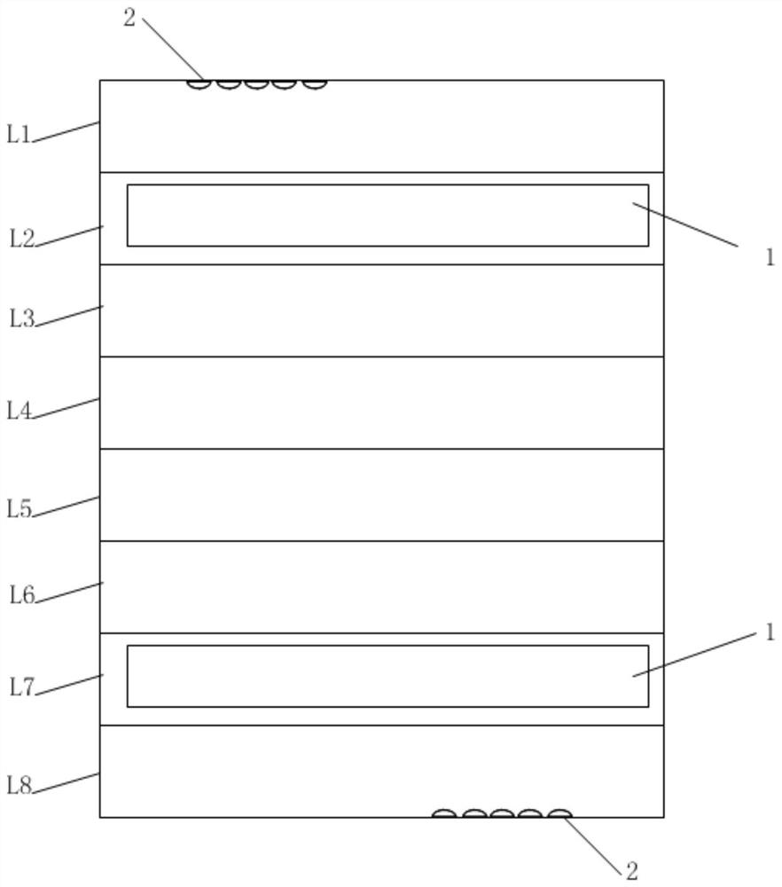
[0087] like Figure 4 As shown, the present invention provides a PCB board for preventing BGA tin cracks, comprising a PCB buffer device 1 and a concave groove pad 2;
[0088] The PCB buffer device 1 is arranged on the GND reflow layer adjacent to the upper surface layer and the lower layer of the PCB to form an elastic GND reflow layer;
[0089] The concave groove pad 2 is arranged at the position of the original BGA pad corresponding to the pin of the BGA chip on the surface of the PCB;
[0090] The concave groove pad includes a groove wall 2.1 and a pad surface 2.2, and the groove wall 2.1 is connected with the pad surface 2.2 to form a cavity 2.3, and an elastic sheet 2.4 is arranged in the cavity 2.3.
[0091] In some embodiments, the PCB buffer device 1 uses a conductive elastic material, and the conductive elastic material can withstand a temperature greater than a temperature threshold; the temperature threshold can be set to 200 degrees.
[0092] In some embodiments...
PUM
 Abstract
Description
Claims
Application Information


