

Dry ice cleaning equipment for semiconductor element
A dry ice cleaning and semiconductor technology, applied in the direction of cleaning methods, cleaning methods and utensils, chemical instruments and methods using gas flow, etc., can solve problems affecting geometric features, waste of resources, failure of integrated circuits, etc., to ensure cleanliness, High cleaning efficiency
- Summary
- Abstract
- Description
- Claims
- Application Information
AI Technical Summary
Problems solved by technology
Method used
Image

Examples
Embodiment
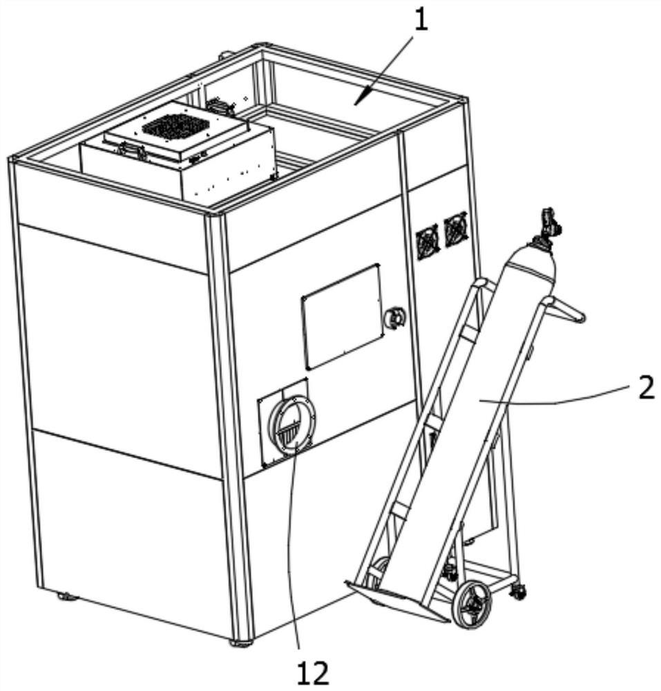
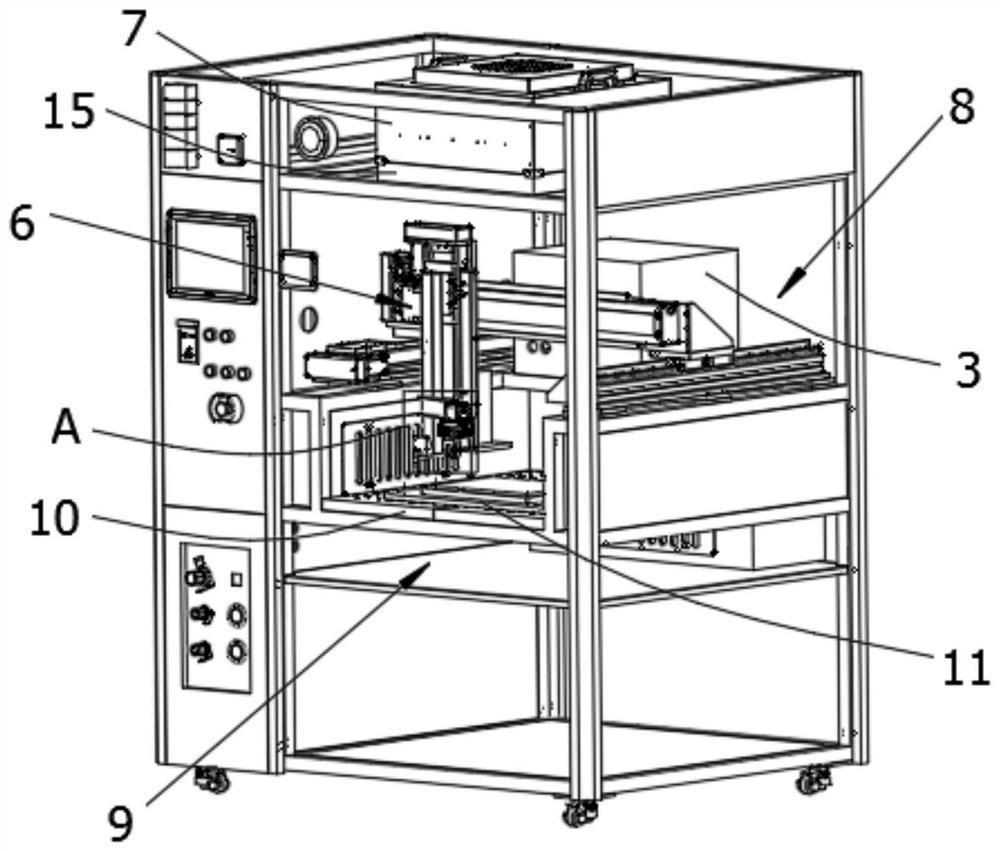
[0026] Embodiment: a kind of semiconductor element is cleaned equipment with dry ice, as Figure 1-Figure 3 As shown, it includes an equipment rack body 1, a dry ice generating mechanism, a dry ice blasting mechanism, a dry ice purification mechanism and a cleaning room installed on the equipment rack body;
[0027] The dry ice generating mechanism includes a liquid carbon dioxide storage tank 2 and a dry ice generator 3, and the liquid carbon dioxide storage tank and the dry ice generator are connected through a hose;
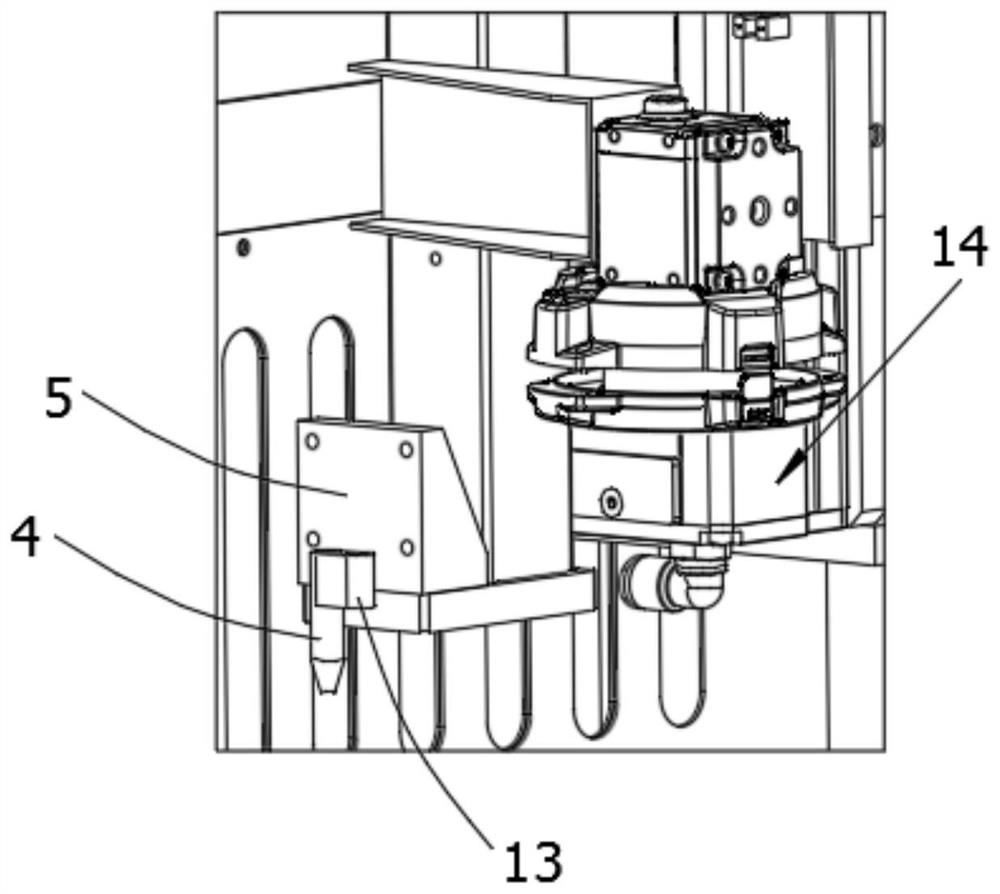
[0028] The dry ice blasting mechanism includes a dry ice nozzle base 5 for installing a dry ice nozzle 4 and a manipulator 6 that drives the dry ice nozzle base to move, the dry ice nozzle is connected to the dry ice generator through a hose, and the dry ice nozzle and the dry ice nozzle The manipulator is located in the cleaning chamber;
[0029] The dry ice purification mechanism includes an intake fan 7 and an exhaust fan, the intake fan is located above t...
PUM
 Abstract
Description
Claims
Application Information