Supercharge Your Innovation With Domain-Expert AI Agents!

Light-emitting diode and manufacturing method thereof

A technology for light-emitting diodes and a manufacturing method, which is applied to semiconductor devices, electrical components, circuits, etc., can solve the problems of mismatch between substrate materials and gallium nitride materials, and long manufacturing cycle of light-emitting diodes, so as to reduce production costs and shorten manufacturing. Cycle time, the effect of improving production efficiency

Pending Publication Date: 2021-04-16
SOUTH UNIVERSITY OF SCIENCE AND TECHNOLOGY OF CHINA
View PDF11 Cites 2 Cited by
  • Summary
  • Abstract
  • Description
  • Claims
  • Application Information

AI Technical Summary

Problems solved by technology

Among them, one of the problems faced by GaN-based light-emitting diodes in the manufacturing process is that the substrate needs to be cleaned and purified in a high temperature and hydrogen atmosphere, and then a buffer layer is deposited on the substrate, which can solve the problem of substrate materials. Mismatch issues with GaN materials
[0003] In the long-term research and development process, the inventors of the present application found that the cleaning and purification process of the substrate needs to be raised to a high temperature for a long time, and then cooled down to the working temperature of the deposited buffer layer after the high temperature has stabilized for a period of time, resulting in the manufacturing of light-emitting diodes. longer period

Method used


Image

  • Light-emitting diode and manufacturing method thereof
  • Light-emitting diode and manufacturing method thereof
  • Light-emitting diode and manufacturing method thereof

Examples


Embodiment Construction

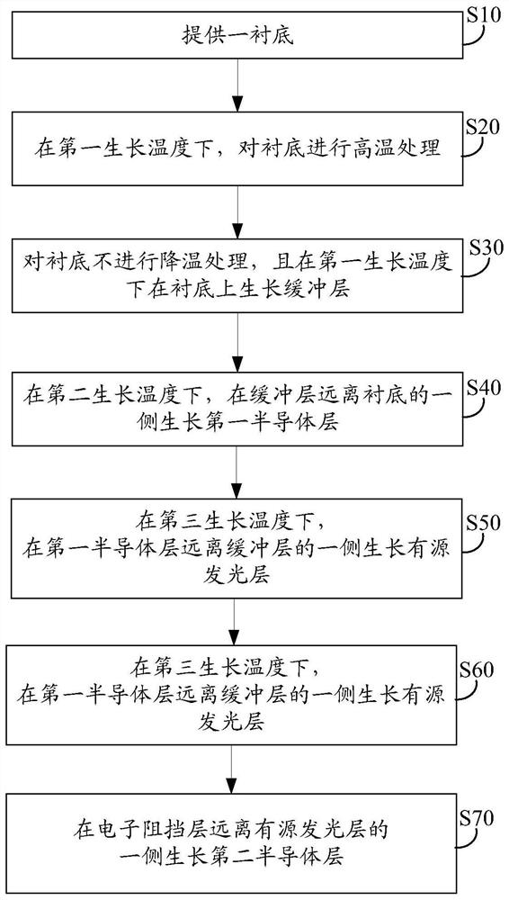
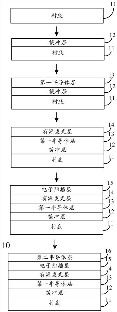
[0013] The following will clearly and completely describe the technical solutions in the embodiments of the present application with reference to the drawings in the embodiments of the present application. Obviously, the described embodiments are only some of the embodiments of the present application, not all of them. Based on the embodiments in this application, all other embodiments obtained by persons of ordinary skill in the art without making creative efforts belong to the scope of protection of this application.

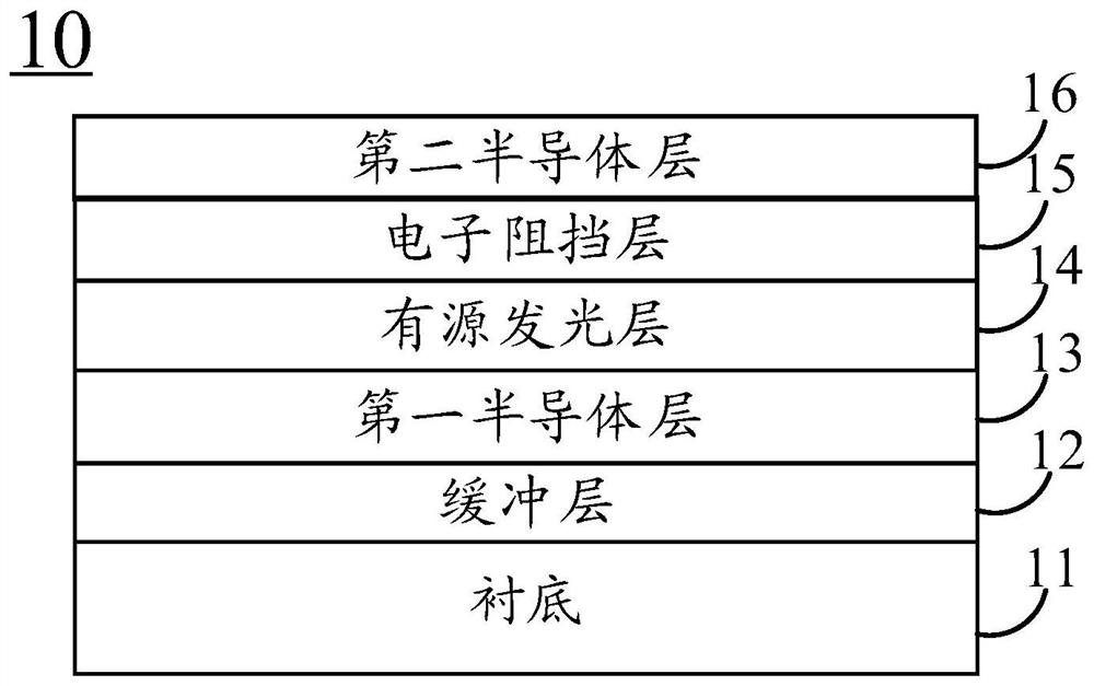
[0014] Such as figure 1 with 2 Shown is a method for manufacturing a light emitting diode 10 according to an embodiment of the present application.

[0015] The manufacturing method of the light emitting diode 10 comprises the following steps:

[0016] S10: providing a substrate 11 .

[0017] It should be noted that the substrate 11 can be a material suitable for the growth of GaN and its semiconductor epitaxial materials, such as sapphire, or it can be a s...


PUM

PropertyMeasurementUnit
Thicknessaaaaaaaaaa
Thicknessaaaaaaaaaa
Thicknessaaaaaaaaaa

Abstract

The invention relates to the field of light-emitting diodes, and particularly discloses a light-emitting diode and a manufacturing method thereof. The method comprises the steps: providing a substrate; carrying out high-temperature treatment on the substrate at a first growth temperature; not cooling the substrate, and growing a buffer layer on the substrate at the first growth temperature; growing a first semiconductor layer on one side, far away from the substrate, of the buffer layer at a second growth temperature; growing an active light-emitting layer on one side, far away from the buffer layer, of the first semiconductor layer at a third growth temperature; growing an electron blocking layer on one side, far away from the first semiconductor layer, of the active light-emitting layer; and growing a second semiconductor layer on one side, away from the active light-emitting layer, of the electron blocking layer. Through the mode, the manufacturing period of the light-emitting diode is shortened, the production cost is reduced, and the production efficiency is improved.

Description

technical field [0001] The present application relates to the field of light-emitting diodes, in particular to a light-emitting diode and a manufacturing method thereof. Background technique [0002] A light emitting diode (Light Emitting Diode, LED) is a semiconductor element that can convert electric current into light in a specific wavelength range. Among them, one of the problems faced by GaN-based light-emitting diodes in the manufacturing process is that the substrate needs to be cleaned and purified in a high temperature and hydrogen atmosphere, and then a buffer layer is deposited on the substrate, which can solve the problem of substrate materials. Mismatch issues with gallium nitride materials. [0003] In the long-term research and development process, the inventors of the present application found that the cleaning and purification process of the substrate needs to be raised to a high temperature for a long time, and then cooled down to the working temperature o...

Claims


Application Information

Patent Timeline
IPC IPC(8): H01L33/00H01L33/12
Inventor 任朝花蒋振宇闫春辉
Owner SOUTH UNIVERSITY OF SCIENCE AND TECHNOLOGY OF CHINA
Features
  • R&D
  • Intellectual Property
  • Life Sciences
  • Materials
  • Tech Scout
  • Unparalleled Data Quality
  • Higher Quality Content
  • 60% Fewer Hallucinations
Learn More