Semiconductor device and erasing and verifying method for semiconductor device
A verification method, semiconductor technology, applied in instruments, static memory, read-only memory, etc., can solve problems such as unfavorable erasure verification accuracy
- Summary
- Abstract
- Description
- Claims
- Application Information
AI Technical Summary
Problems solved by technology
Method used
Image

Examples
Embodiment 1
[0063] Embodiments of the present application provide an erasing and verifying method for a semiconductor device.
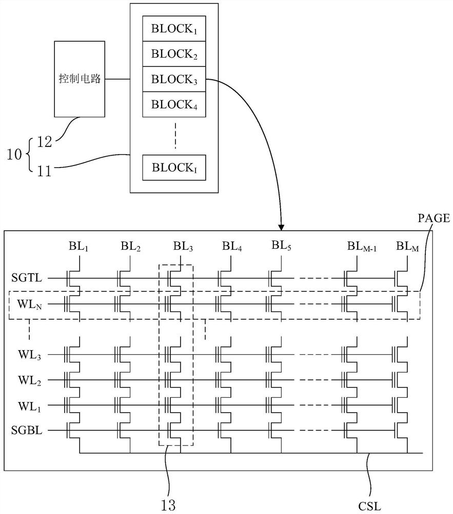
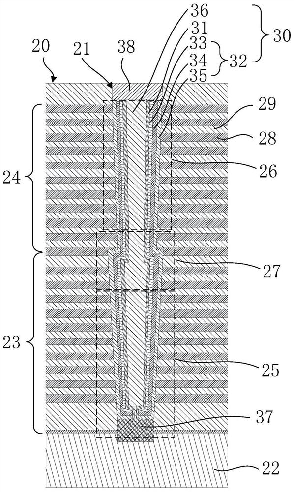
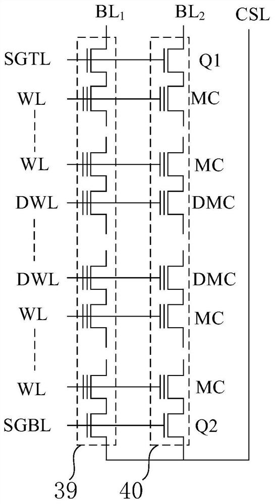
[0064] Specifically, combine Figure 1 to Figure 3 As shown, semiconductor device 20 is a three-dimensional memory device, such as 3D NAND memory device 10 . The semiconductor device 20 includes a plurality of memory blocks BLOCK, and selected ones of the plurality of memory blocks include a plurality of memory cell strings 21, eg, a plurality of NAND strings. like image 3 As shown, each memory cell string 21 includes a top select transistor Q1, a bottom select transistor Q2, a plurality of memory cells MC and at least one dummy memory cell DMC arranged in series. In this embodiment, the number of virtual storage units DMC is multiple, but not limited to this. Among them, a plurality of memory cells MC and a plurality of dummy memory cells DMC are located between the top selection transistor Q1 and the bottom selection transistor Q2. The plurality of dummy m...
Embodiment 2
[0090]The embodiment of the present application also provides an erasing and verification method for a semiconductor device, which is different from the above-mentioned embodiment in step S402. This embodiment can solve the negative impact of incomplete erasing on the verification process of selected memory cell strings.
[0091] In this embodiment, in the verification operation phase, the verification operation phase is divided into a pre-conduction phase and a verification phase in turn; in the pre-conduction phase, a selected memory cell string in the plurality of memory cell strings is set as a channel On state; during the verification phase, the threshold voltages of selected memory cells in the selected memory cell strings are verified; and throughout the verification operation phase, the unselected memory cell strings are set to the channel-off state.
[0092] Specifically, combine image 3 , Figure 7 and Figure 8 As shown, in the whole verification operation stage...
Embodiment 3
[0098] The embodiment of the present application also provides an erasing and verification method for a semiconductor device, which is different from the above-mentioned embodiment in step S402. This embodiment can solve the influence of the strong electric field generated by the first turn-on voltage Vpass1 on the dummy word line of the dummy memory cell DMC on the unselected memory cell string.
[0099] In this embodiment, in the verification operation stage, the verification operation stage is divided into a pre-conduction stage and a verification stage in turn; in the pre-conduction stage, unselected memory cell strings in the plurality of memory cell strings are set as channel In the verification stage, the unselected memory cell strings are set to the channel off state, and the selected memory cell strings are set to the channel off state. The threshold voltages of selected memory cells in the memory cell string are verified.
[0100] Specifically, combine image 3 , ...
PUM
 Abstract
Description
Claims
Application Information
 - R&D
- Intellectual Property
- Life Sciences
- Materials
- Tech Scout
- Unparalleled Data Quality
- Higher Quality Content
- 60% Fewer Hallucinations
Browse by: Latest US Patents, China's latest patents, Technical Efficacy Thesaurus, Application Domain, Technology Topic, Popular Technical Reports.
© 2025 PatSnap. All rights reserved.Legal|Privacy policy|Modern Slavery Act Transparency Statement|Sitemap|About US| Contact US: help@patsnap.com