Unlock instant, AI-driven research and patent intelligence for your innovation.

Semiconductor device and method for erasing and verifying semiconductor device

A verification method and semiconductor technology, applied in instruments, static memory, read-only memory, etc., can solve problems such as unfavorable erasure verification accuracy, and achieve the effect of avoiding HCI risks and improving accuracy

Active Publication Date: 2022-04-29
YANGTZE MEMORY TECH CO LTD
View PDF7 Cites 0 Cited by
  • Summary
  • Abstract
  • Description
  • Claims
  • Application Information

AI Technical Summary

Problems solved by technology

However, when erasing memory cells in a NAND string, there is a risk of HCI (Hot Carrier Injection), which is not conducive to improving the accuracy of erase verification

Method used


Image

  • Semiconductor device and method for erasing and verifying semiconductor device
  • Semiconductor device and method for erasing and verifying semiconductor device
  • Semiconductor device and method for erasing and verifying semiconductor device

Examples


Embodiment 1

[0063] An embodiment of the present application provides a method for erasing and verifying a semiconductor device.

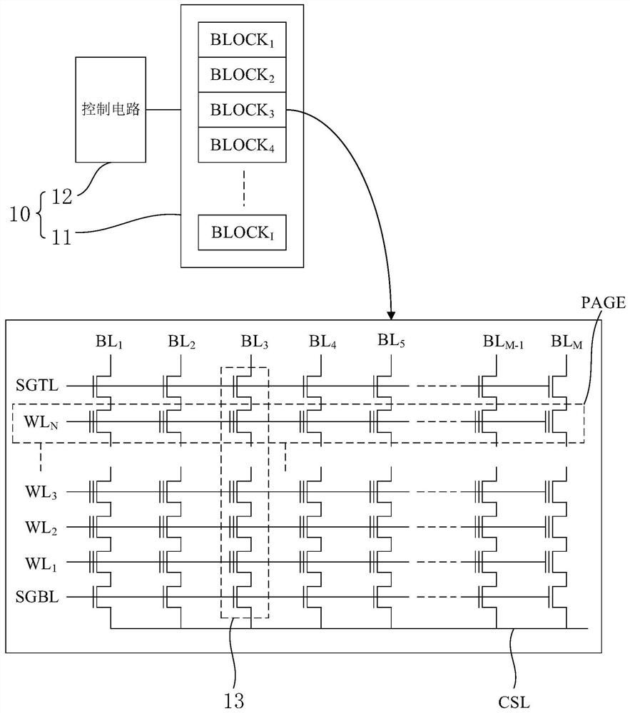
[0064] Specifically, combine Figure 1 to Figure 3 As shown, the semiconductor device 20 is a three-dimensional memory device, such as the 3D NAND memory device 10 . The semiconductor device 20 includes a plurality of memory blocks BLOCK, and a selected one of the plurality of memory blocks includes a plurality of memory cell strings 21, such as a plurality of NAND strings. Such as image 3 As shown, each memory cell string 21 includes a top selection transistor Q1, a bottom selection transistor Q2, a plurality of memory cells MC and at least one dummy memory cell DMC arranged in series. In this embodiment, there are multiple virtual storage units DMC, but it is not limited thereto. Wherein, a plurality of memory cells MC and a plurality of dummy memory cells DMC are located between the top selection transistor Q1 and the bottom selection transistor Q2. A p...

Embodiment 2

[0090]The embodiment of the present application also provides a method for erasing and verifying a semiconductor device, which is different from the above embodiments in step S402. This embodiment can solve the negative impact of incomplete erasing on the verification process of the selected memory cell string.

[0091] In this embodiment, in the verification operation phase, the verification operation phase is sequentially divided into a pre-conduction phase and a verification phase; in the pre-conduction phase, a selected memory cell string among a plurality of memory cell strings is set as a channel In the conduction state; in the verification phase, the threshold voltage of the selected memory cell in the selected memory cell string is verified; and in the whole verification operation phase, the unselected memory cell string is set to the channel cut-off state.

[0092] Specifically, combine image 3 , Figure 7 and Figure 8 As shown, in the entire verification operati...

Embodiment 3

[0098] The embodiment of the present application also provides a method for erasing and verifying a semiconductor device, which is different from the above embodiments in step S402. This embodiment can solve the influence of the strong electric field generated by the first conduction voltage Vpass1 on the dummy word line of the dummy memory cell DMC on the unselected memory cell strings.

[0099] In this embodiment, in the verification operation stage, the verification operation stage is divided into a pre-conduction stage and a verification stage in sequence; channel conduction state, and set the selected memory cell strings in the channel cut-off state among the plurality of memory cell strings; The threshold voltage of the selected memory cell in the memory cell string is verified.

[0100] Specifically, combine image 3 , Figure 9 and Figure 10 As shown, in the entire verification operation phase (T2 to T4 period, including the pre-conduction phase and the verificati...


PUM


Abstract

The application discloses a semiconductor device and a method for erasing and verifying the semiconductor device. The semiconductor device includes a plurality of memory blocks, and a selected memory block in the plurality of memory blocks includes a plurality of memory cell strings, and each memory cell string Including a plurality of memory cells; erasing and verification methods include: in the erasing operation phase, erasing a plurality of memory cells in each memory cell string; in the verification operation phase, including the pre-conduction phase and the verification phase, multiple storage The cell strings include selected memory cell strings and unselected memory cell strings; in the pre-conduction stage, at least one of the selected memory cell strings and unselected memory cell strings is set to a channel conduction state; In the verification stage, the threshold voltage of at least one memory cell in the selected memory cell string is verified, and the unselected memory cell string is set to a channel cut-off state. The present application can avoid the risk of hot carrier injection, and is beneficial to improving the accuracy of erasing verification of semiconductor devices.

Description

technical field [0001] The present application relates to a semiconductor device and its erasing and verification method, in particular to a semiconductor device capable of avoiding the risk of hot carrier injection and an erasing and verification method for the semiconductor device. Background technique [0002] Semiconductor memory is widely used in various electronic devices, such as cellular telephones, digital cameras, personal digital assistants, medical electronic devices, mobile computing devices, and non-mobile computing devices. Non-volatile memory allows information to be stored and preserved. Examples of nonvolatile memory include flash memory (eg, NAND type and NOR type flash memory) and electrically erasable programmable read only memory (Electrically Erasable Programmable Read Only Memory, EEPROM). [0003] Recently, ultra-high density memory devices using three-dimensional (3D) stacked memory structures, sometimes referred to as bit-cost scalable (BiCS) arch...

Claims


Application Information

Patent Timeline
Patent Type & Authority Patents(China)
IPC IPC(8): G11C16/34G11C16/04G11C16/14
CPCG11C16/3445G11C16/14G11C16/0483
Inventor 贾建权李达游开开李楷威罗哲田瑶瑶刘畅李姗张安靳磊
Owner YANGTZE MEMORY TECH CO LTD