Read operating circuit, semiconductor memory, and read operating method

A read operation, semiconductor technology, applied in the field of read operation circuit, to achieve the effect of reducing power consumption, compressing current, and reducing the number of flips

Pending Publication Date: 2021-04-27
CHANGXIN MEMORY TECH (SHANGHAI) INC
View PDF0 Cites 4 Cited by
  • Summary
  • Abstract
  • Description
  • Claims
  • Application Information

AI Technical Summary

Problems solved by technology

[0005] The embodiment of the present application provides a read operation circuit, a semiconductor memory and a read operation method to solve or alleviate one or more technical problems in the prior art

Method used


Image

  • Read operating circuit, semiconductor memory, and read operating method
  • Read operating circuit, semiconductor memory, and read operating method
  • Read operating circuit, semiconductor memory, and read operating method

Examples


Embodiment Construction

[0079] Example embodiments will now be described more fully with reference to the accompanying drawings. Example embodiments may, however, be embodied in many forms and should not be construed as limited to the embodiments set forth herein; rather, these embodiments are provided so that this application will be thorough and complete, and will fully convey the concept of example embodiments to those skilled in the art. The same reference numerals denote the same or similar parts in the drawings, and thus their repeated descriptions will be omitted.

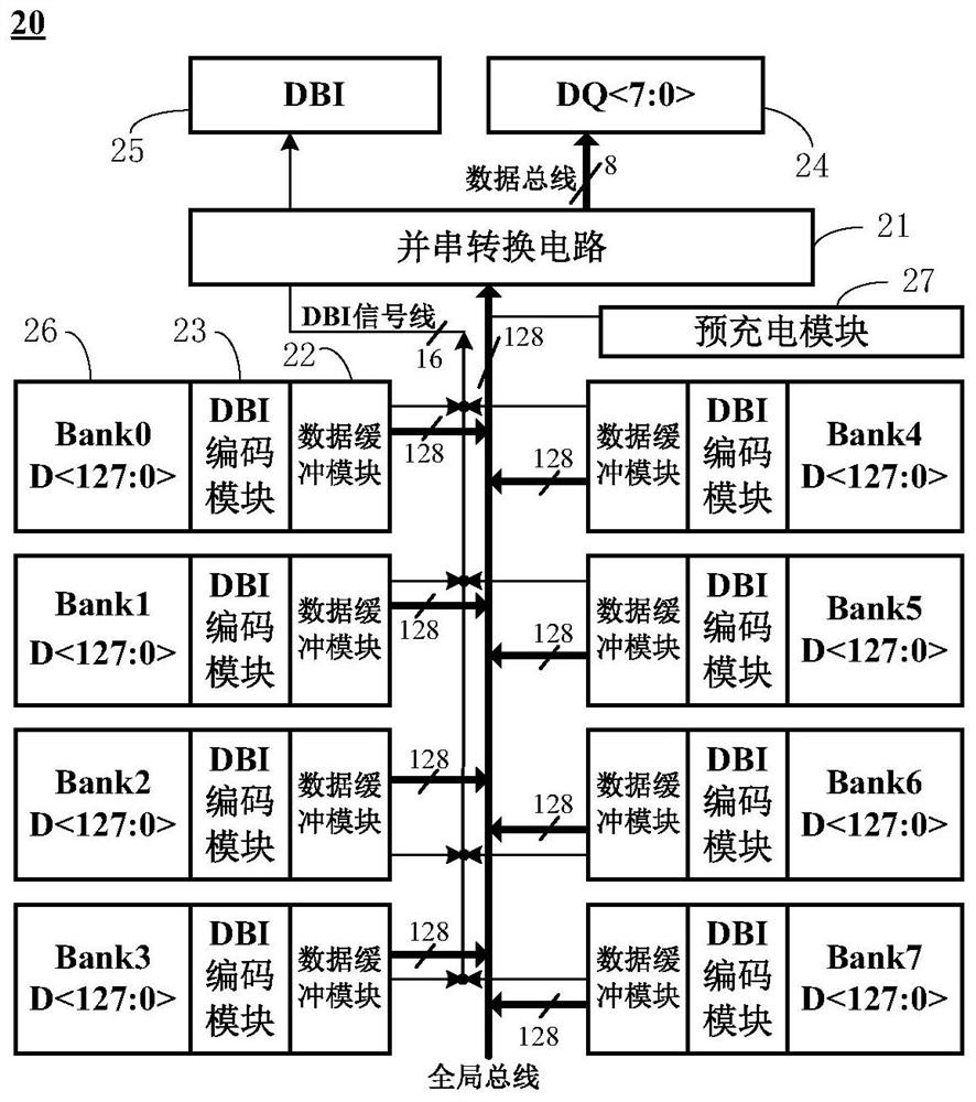
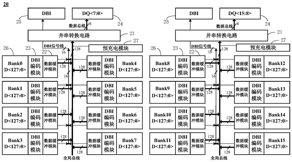
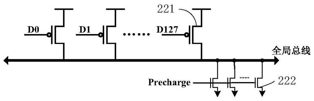
[0080] figure 1 A block diagram schematically showing a partial structure of a semiconductor memory in an implementation manner of this embodiment. Such as figure 1 As shown, the semiconductor memory 20 includes a DQ port 24 , a data line inversion (Data Bus Inversion, DBI) port 25 , a storage block (Bank) 26 and a read operation circuit. Wherein, the read operation circuit includes a global bus (Global Bus), a DBI signal line,...


PUM


Abstract

The embodiment of the invention at least provides a read operation circuit. Theread operation circuit comprises: a DBI encoding module which is used for reading read data from a storage block and determining whether to overturn the read data according to the digit of the data which is high in the read data so as to output global bus data transmitted by a global bus and DBI data transmitted by a DBI signal line, and a DBI port used for receiving the DBI data; a parallel-serial conversion circuit which is used for carrying out parallel-serial conversion on the global bus data so as to generate output data of the DQ port; a data buffer module which is connected to the storage block through a global bus; and a pre-charging module which is connected to the pre-charging signal line and is used for setting the initial state of the global bus to be low. According to the technical scheme of the embodiment of the invention, more '0' data can be transmitted on the global bus of the Precharge pull-down architecture, so that the turnover frequency of the internal global bus can be reduced, the current is greatly compressed, and the power consumption is reduced.

Description

technical field [0001] The present application relates to the technical field of semiconductor memory, and in particular to a read operation circuit, a semiconductor memory and a read operation method. Background technique [0002] This section is intended to provide a background or context to embodiments of the application that are recited in the claims. The descriptions herein are not admitted to be prior art by inclusion in this section. [0003] Semiconductor memory includes Static Random-Access Memory (SRAM for short), Dynamic Random Access Memory (Dynamic Random Access Memory, DRAM for short), Synchronous Dynamic Random Access Memory (Synchronous Dynamic Random Access Memory, SDRAM for short) , read-only memory (Read-Only Memory, ROM for short), flash memory, and the like. [0004] In the DRAM protocol of the Joint Electron Device Engineering Council (JEDEC), there are specific requirements for the speed and power saving of DRAM. How to make DRAM more power-saving w...

Claims


Application Information

Patent Timeline
Patent Type & Authority Applications(China)
IPC IPC(8): G11C11/4093G11C11/4096
CPCG11C11/4093G11C11/4096G11C2207/107G11C7/1006G11C7/02G11C7/1048G11C7/1015G11C7/1057G11C7/1084G11C11/4091G11C11/4097G11C7/1051
Inventor 张良
Owner CHANGXIN MEMORY TECH (SHANGHAI) INC
Why Eureka
Try Eureka