Semiconductor terminal structure and preparation method thereof

A terminal structure, semiconductor technology, applied in the direction of semiconductor/solid-state device manufacturing, semiconductor devices, electrical components, etc., can solve the problem of poor concentration gradient gradient effect

Pending Publication Date: 2021-04-27
GREE ELECTRIC APPLIANCES INC +1
View PDF0 Cites 1 Cited by
  • Summary
  • Abstract
  • Description
  • Claims
  • Application Information

AI Technical Summary

Problems solved by technology

IGBT terminals usually use field-limiting ring technology to improve the high-voltage performance of IGBT. At present, the commonly used field-limiting ring technology is to introduce one or more doping types opposite to the silicon substrate at the power semiconductor terminal, but the concentration is much higher than that of the substrate. The ring-shaped area is used to increase the breakdown voltage; but the above-mentioned method has the problem of poor concentration gradient gradient effect

Method used


Image

  • Semiconductor terminal structure and preparation method thereof
  • Semiconductor terminal structure and preparation method thereof
  • Semiconductor terminal structure and preparation method thereof

Examples


Embodiment Construction

[0044] In order to more clearly illustrate the technical solutions of the embodiments of the present application, the accompanying drawings used in the embodiments will be briefly introduced below. It should be understood that the following drawings only show some embodiments of the present invention, and therefore are not It should be regarded as a limitation on the scope, and those skilled in the art can also obtain other related drawings based on these drawings without creative work.

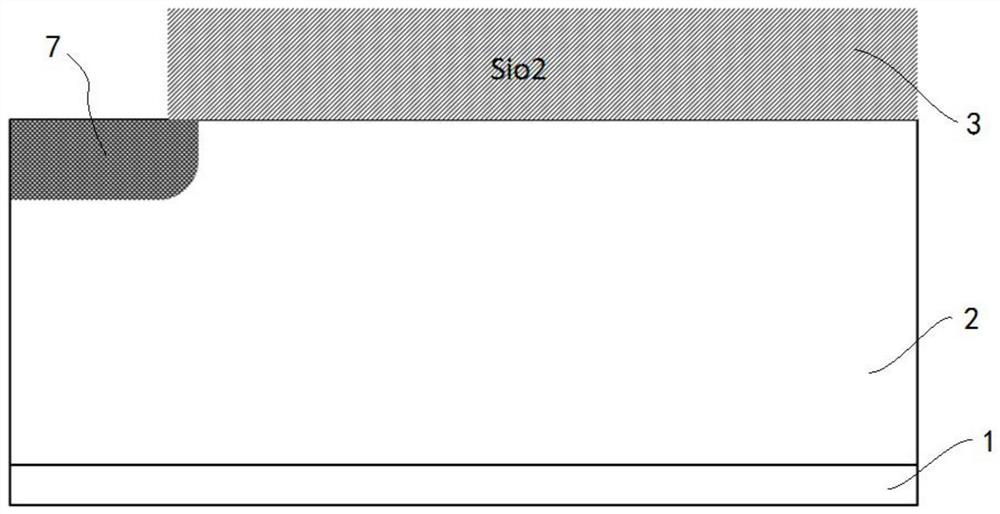
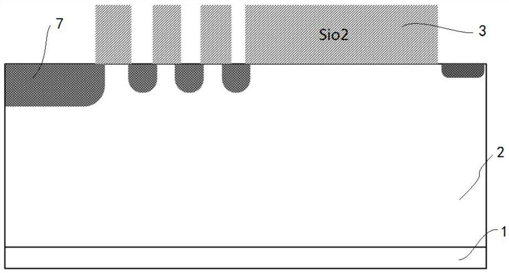
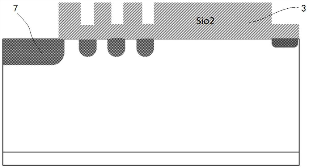
[0045] A semiconductor structure provided by Embodiment 1 of the present invention, such as Figure 9 As shown, it includes a semiconductor terminal structure and a main junction 7, wherein the semiconductor terminal structure is an IGBT terminal structure, which includes: a substrate layer 1 and an epitaxial layer 2 disposed on the substrate layer 1, an oxide layer is grown on the epitaxial layer 2; A plurality of junction terminal extension structures 5 are formed on the layer 2, and the ju...


PUM


Abstract

The invention provides a semiconductor terminal structure and a preparation method thereof. The preparation method comprises the following steps of growing an epitaxial layer on a substrate layer, growing a first oxide layer with a preset thickness on the epitaxial layer, etching the first oxide layer to form a plurality of junction terminal injection ports which are distributed in a step shape along a preset direction, and injecting ions through the junction terminal injection ports, so that a plurality of junction terminal expansion structures which are distributed at intervals along a preset direction and of which the concentrations are decreased progressively are formed on the epitaxial layer. By etching the first oxide layer, a plurality of junction terminal injection ports which are distributed in a step shape along the preset direction can be formed, and the junction terminal injection ports are distributed in a step shape of which the heights are sequentially increased, so that the depths of the junction terminal injection ports on the first oxide layer are different; and the depths of the injected ions diffused to the epitaxial layer from the junction terminal injection ports with different depths are sequentially reduced, so that different junction terminal expansion structures of which the concentration gradients are progressively changed are formed, and the gradual change effect of the concentration gradients is good.

Description

technical field [0001] The invention relates to the technical field of semiconductors, in particular to a semiconductor terminal structure and a preparation method thereof. Background technique [0002] IGBT (Insulated Gate Bipolar Transistor) is a semiconductor power device that combines MOSFET (Metal Oxide Field Effect Transistor) and BJT (Bipolar Transistor), with high input impedance, low switching loss, fast speed, voltage drive Features such as low power. IGBT terminals usually use field-limiting ring technology to improve the high-voltage performance of IGBT. At present, the commonly used field-limiting ring technology is to introduce one or more doping types opposite to the silicon substrate at the power semiconductor terminal, but the concentration is much higher than that of the substrate. The ring-shaped area is used to increase the breakdown voltage; but the above-mentioned method has the problem of poor concentration gradient gradient effect. Contents of the ...

Claims


Application Information

Patent Timeline
Patent Type & Authority Applications(China)
IPC IPC(8): H01L29/739H01L21/331H01L29/06
CPCH01L29/0603H01L29/66325H01L29/7393
Inventor 刘勇强张祎龙曾丹史波
Owner GREE ELECTRIC APPLIANCES INC
Why Eureka
Try Eureka