Photosensitive element and preparation method thereof, and display device

A technology for photosensitive elements and display devices, which is applied in the direction of electrical components, semiconductor devices, and electric solid-state devices, can solve the problems of high cost and low hole transmission efficiency, improve performance, improve hole transmission efficiency, and reduce preparation requirements Effect

Active Publication Date: 2022-07-12
TCL CHINA STAR OPTOELECTRONICS TECH CO LTD
View PDF4 Cites 0 Cited by
  • Summary
  • Abstract
  • Description
  • Claims
  • Application Information

AI Technical Summary

Problems solved by technology

[0004] The invention provides a photosensitive element, a preparation method thereof, and a display device, which are used to solve the technical problems of high cost and low hole transport efficiency caused by the use of P-type materials in the photosensitive element in the prior art

Method used


Image

  • Photosensitive element and preparation method thereof, and display device
  • Photosensitive element and preparation method thereof, and display device
  • Photosensitive element and preparation method thereof, and display device

Examples


Embodiment Construction

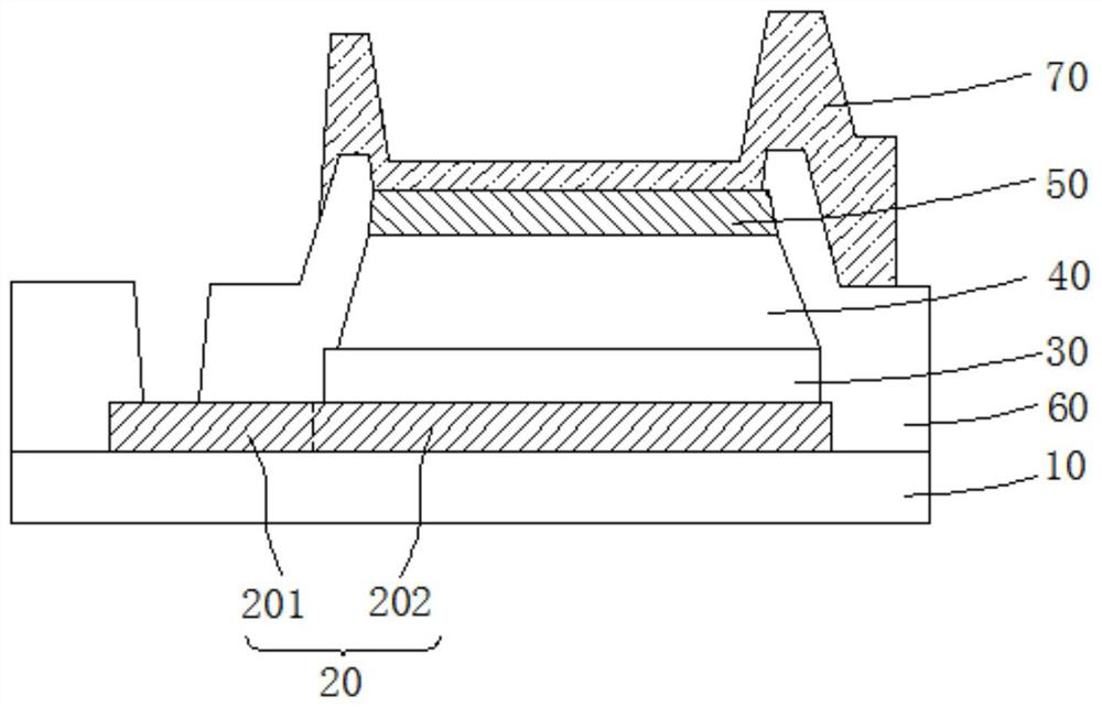
[0053] The technical solutions in the embodiments of the present invention will be clearly and completely described below with reference to the accompanying drawings in the embodiments of the present invention. Obviously, the described embodiments are only some, but not all, embodiments of the present invention. Based on the embodiments of the present invention, all other embodiments obtained by those skilled in the art without creative efforts shall fall within the protection scope of the present invention.

[0054] In the description of the present invention, it should be understood that the terms "portrait", "horizontal", "length", "width", "upper", "lower", "front", "rear", "left", " The orientation or positional relationship indicated by "right", "vertical", "horizontal", etc. is based on the orientation or positional relationship shown in the drawings, and is only for the convenience of describing the present invention and simplifying the description, rather than indicat...


PUM

PropertyMeasurementUnit
electron work functionaaaaaaaaaa

Abstract

The present invention provides a photosensitive element, a preparation method thereof, and a display device. The photosensitive element comprises: a substrate; a first electrode disposed on the substrate; an N-type doped silicon layer disposed on the first electrode a non-doped silicon layer, arranged on the N-type doped silicon layer; a molybdenum oxide layer, arranged on the non-doped silicon layer; an insulating layer, arranged on the molybdenum oxide layer and the substrate , the insulating layer is provided with a first opening to expose the molybdenum oxide layer; a second electrode is arranged on the insulating layer and the molybdenum oxide layer, and passes through the first opening and the molybdenum oxide layer touch. The photosensitive element provided by the present invention adopts the molybdenum oxide layer with high work function to replace the P-type material of the homojunction or heterojunction structure in the prior art, which not only saves the cost, but also can improve the hole transport efficiency of the photosensitive element, thereby improving the photosensitive element. component performance.

Description

technical field [0001] The present invention relates to the field of display technology, and in particular, to a photosensitive element, a preparation method thereof, and a display device. Background technique [0002] With the development of technology, the use of fingerprint, voice, face, hand, retina or iris as a personal identification system has become a safe and reliable biometric technology. In terms of cost, ease of use and accuracy, fingerprint recognition has become the leading method for verifying identity, replacing conventional passwords and keys. The photosensitive element in the traditional fingerprint recognition optical sensor has problems such as high cost, large volume and image distortion. Photosensitive elements based on silicon chips are favored because they can be made very small and cheap. However, the structure of photosensitive elements based on silicon chips usually needs to use P-type materials to form homojunction or heterojunction structures, ...

Claims


Application Information

Patent Timeline
Patent Type & Authority Patents(China)
IPC IPC(8): H01L31/109H01L31/0224H01L31/18H01L27/32
CPCH01L31/109H01L31/022408H01L31/1804H10K59/60Y02P70/50H01L31/0336H01L31/105H01L31/18G06F3/0412H01L27/14603H01L27/14607H01L27/14612H01L27/14678H01L31/0264
Inventor 蔡广烁
Owner TCL CHINA STAR OPTOELECTRONICS TECH CO LTD
Why Eureka
Try Eureka