

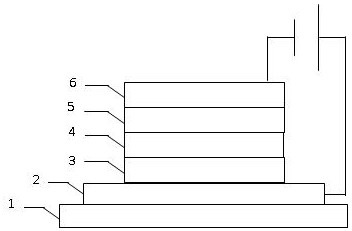
A quantum dot light-emitting diode and its preparation method
A quantum dot light-emitting and diode technology, which is applied in semiconductor/solid-state device manufacturing, semiconductor devices, electrical components, etc., can solve the problems of low hole transmission efficiency, poor device performance, and uneven hole-electron charge transmission, etc., to achieve Effects of improving hole transport efficiency, improving luminous efficiency, and improving hole mobility
- Summary
- Abstract
- Description
- Claims
- Application Information
AI Technical Summary
Problems solved by technology
Method used
Image

Examples
Embodiment 1
[0048] Embodiment 1: The following takes the preparation of a hole transport layer using molybdenum oxide and initial black phosphorus nanomaterials as an example for a detailed introduction:
[0049] Put the initial black phosphorus nanomaterials in the air and irradiate them with ultraviolet light for 4 minutes to prepare black phosphorus nanomaterials, then disperse molybdenum oxide with a particle size below 100nm in ethanol (80mg / mL) and stir well, and take the thickness Black phosphorus nanomaterials with a size below 10nm are uniformly dispersed in molybdenum oxide ethanol solution, wherein the mass ratio of black phosphorus nanomaterials to molybdenum oxide is 2.0%, stirred at a rate of 3000rpm / min for 30 minutes until the solution is completely uniform, and prepared mixed solution;
[0050] The mixed solution was spin-coated on the anode substrate, heated to 150° C. on a heating platform and kept for 15 minutes to form a hole transport layer.
Embodiment 2
[0051] Embodiment 2: The following uses tungsten oxide and initial black phosphorus nanomaterials to prepare a black hole transport layer as an example for detailed introduction:
[0052] Place the initial black phosphorus nanomaterials in the air and irradiate them with ultraviolet light for 3 minutes to prepare black phosphorus nanomaterials, then disperse tungsten oxide with a particle size below 100nm in methanol (100mg / mL) and stir thoroughly, and take the thickness Black phosphorus nanomaterials below 10nm are uniformly dispersed in tungsten oxide methanol solution, wherein the mass ratio of black phosphorus nanomaterials to tungsten oxide is 2.0%, stirred at a rate of 3000rpm / min for 30 minutes until the solution is completely uniform, and a mixed liquid;
[0053] The mixed solution was spin-coated on the anode substrate, heated to 150° C. on a heating platform and kept for 15 minutes to form a hole transport layer.
Embodiment 3
[0054] Embodiment 3: The following takes the use of nickel oxide and initial black phosphorus nanomaterials to prepare a hole transport layer as an example for detailed introduction:
[0055] Put the initial black phosphorus nanomaterials in the air and irradiate them with ultraviolet light for 5 minutes to prepare the black phosphorus nanomaterials, then disperse nickel oxide with a particle size below 100nm in ethanol (60mg / mL) and stir well, take Black phosphorus nanomaterials with a thickness of less than 10nm are uniformly dispersed in a nickel oxide solution, wherein the mass ratio of black phosphorus nanomaterials to nickel oxide is 2.0%, and stirred at a rate of 3000rpm / min for 30 minutes until the solution is completely uniform. mixed solution;
[0056] The mixed solution was spin-coated on the anode substrate, heated to 110° C. on a heating platform and kept for 15 minutes to form a hole transport layer.
[0057] In summary, the present invention provides a quantum ...
PUM
| Property | Measurement | Unit |
|---|---|---|
| particle diameter | aaaaa | aaaaa |
| thickness | aaaaa | aaaaa |
| particle diameter | aaaaa | aaaaa |
Abstract
Description
Claims
Application Information