Organic electroluminescence device and preparation method thereof

An electroluminescence device and an electroluminescence technology, which are applied in the field of electric light sources, can solve the problems of unsatisfactory luminous efficiency of the light-emitting device, low carrier transport efficiency, uneven doping of the transport layer, etc., and achieve the hole transport layer by layer. The structure is uniform and stable, the effect of improving hole transport efficiency and improving luminous efficiency

Inactive Publication Date: 2014-06-11
OCEANS KING LIGHTING SCI&TECH CO LTD +2
View PDF7 Cites 0 Cited by
  • Summary
  • Abstract
  • Description
  • Claims
  • Application Information

AI Technical Summary

Problems solved by technology

However, at present, the transport layer obtained by doping is unevenly doped, the internal resistance is still large, the carrier transport efficiency is low, and the required start-up voltage is high, resulting in unsatisfactory luminous efficiency of organic electroluminescent devices and long life. short

Method used


Image

  • Organic electroluminescence device and preparation method thereof
  • Organic electroluminescence device and preparation method thereof
  • Organic electroluminescence device and preparation method thereof

Examples


preparation example Construction

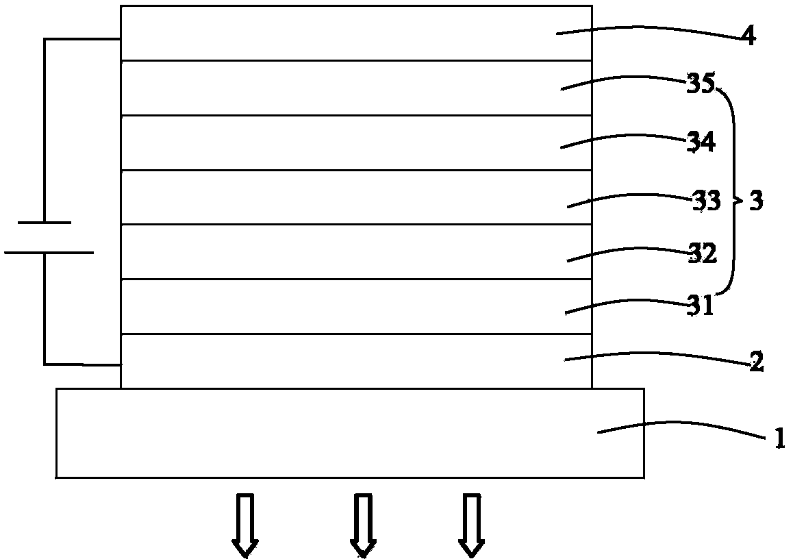
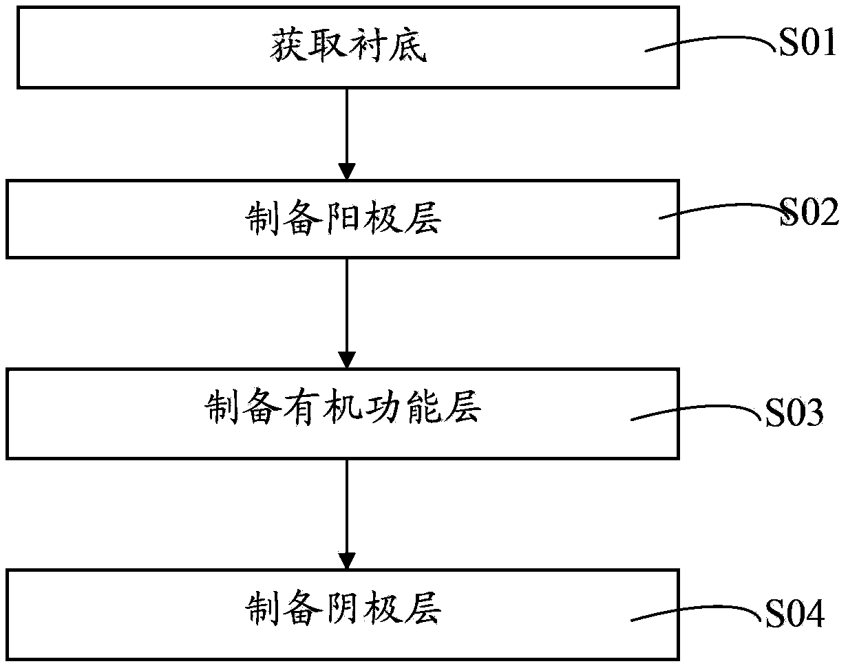
[0029] Correspondingly, the embodiment of the present invention also provides a method for preparing the above-mentioned organic electroluminescent device. The process of the preparation method is as follows figure 2 shown, please also see figure 1 , including the following steps:

[0030] S01. Obtain the substrate: obtain the substrate of the required size according to actual needs as the substrate layer 1;

[0031] S02. Prepare the anode layer 2: plate the anode layer 2 on one surface of the substrate layer 1;

[0032] S03. Preparation of organic functional layer 3: the surface of the anode layer 2 prepared in step S02 opposite to the substrate layer 1 is coated with an organic functional layer 3, wherein the organic functional layer 3 includes a hole transport layer 31 and an external power supply The light-emitting layer 33 that emits light under driving, the hole transport layer 31 is stacked and combined between the anode layer 2 and the light-emitting layer 33, wher...
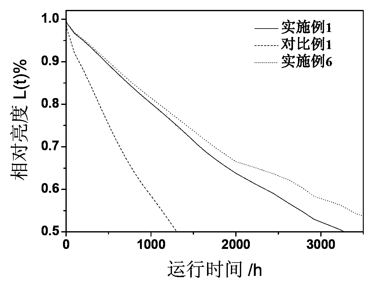
Embodiment 1

[0044] An organic electroluminescence device, its structure is glass substrate / ITO (100nm) / CuI:CuPc (20nm) / TAPC (10nm) / DCJTB:Alq 3 (20nm) / BAlq(10nm) / Cs 2 CO 3 :TPBi(20nm) / Al(100nm). Among them, the hole transport layer is a mixture layer of CuI and CuPc doped with each other, and the doping mass percentage of CuI in the hole transport layer is 2%; the electron transport layer is Cs 2 CO 3 Interdoped mixture layer with TPBi, and Cs 2 CO 3 The mass percentage of doping in the electron transport layer was 2%.

[0045] The preparation method of the organic electroluminescence device comprises the following steps:

[0046] Step S11. Provide a glass substrate: place the glass substrate in deionized water containing detergent for ultrasonic cleaning, and after cleaning, use isopropanol and acetone in ultrasonic treatment for 20 minutes, and then dry it with nitrogen for use;

[0047] Step S12. In the magnetron sputtering system, prepare an ITO anode layer on the glass substrat...

Embodiment 2

[0053] An organic electroluminescence device, its structure is glass substrate ITO (100nm) / CuI:ZnPc (40nm) / TAPC (10nm) / DCJTB:Alq 3 (20nm) / BAlq(10nm) / Li 2 CO 3 : BPhen(40nm) / Al(100nm). Wherein, the hole transport layer is a mixture layer of CuI and ZnPc doped with each other, and the doping mass percentage of CuI in the hole transport layer is 5%; the electron transport layer is Li 2 CO 3 Interdoped mixture layer with BPhen, and Li 2 CO 3 The mass percentage of doping in the electron transport layer was 5%.

[0054] The preparation method of the organic electroluminescent device comprises the following steps:

[0055] Step S21. Provide a glass substrate: place the glass substrate in deionized water containing detergent for ultrasonic cleaning, and after cleaning, use isopropanol and acetone in ultrasonic treatment for 20 minutes, and then dry it with nitrogen for use;

[0056] Step S22. In the magnetron sputtering system, prepare an ITO anode layer on the glass substrate...


PUM


Abstract

The invention discloses an organic electroluminescence device and a preparation method thereof. The organic electroluminescence device comprises a substrate layer, an anode layer, an organic functional layer and a cathode layer which are laminated and combined in turn. The organic functional layer comprises a hole transmission layer and a light-emitting layer which is driven to emit light by an external power supply. The hole transmission layer is laminated and combined between the anode layer and the light-emitting layer. Mass percentage of 12-10% of cuprous iodide is doped in the hole transmission layer. The preparation method of the organic electroluminescence device comprises steps that a substrate is acquired, the anode layer is prepared, the organic functional layer is prepared and the cathode layer is prepared, etc. The organic electroluminescence device is high in light emission efficiency, low in starting voltage and long in the service life. The preparation method of the organic electroluminescence device is simple in technology, conditions are easy to control and product qualified rate is high so that production efficiency is effectively enhanced, and thus the organic electroluminescence device is suitable for industrialized production.

Description

technical field [0001] The invention belongs to the technical field of electric light sources, and in particular relates to an organic electroluminescent device and a preparation method thereof. Background technique [0002] Organic Light Emission Diode (hereinafter referred to as OLED) has the characteristics of high brightness, wide range of material selection, low driving voltage, full-cured active light emission, etc., and has the advantages of high definition, wide viewing angle, and fast response speed. A display technology and light source with great potential, in line with the development trend of mobile communication and information display in the information age, and the requirements of green lighting technology, is the focus of many researchers at home and abroad. [0003] The organic electroluminescent device is a carrier-injection light-emitting device. After the anode and the cathode are applied with an operating voltage, holes are injected from the anode and e...

Claims


Application Information

Patent Timeline
Patent Type & Authority Applications(China)
IPC IPC(8): H01L51/50H01L51/54H01L51/56
CPCH10K50/155H10K2102/00H10K71/00
Inventor 周明杰王平冯小明张振华
Owner OCEANS KING LIGHTING SCI&TECH CO LTD
Why Eureka
Try Eureka