Applied to electrical connectors, electrostatic chucks and semiconductor devices in vacuum chambers
An electrical connector and vacuum chamber technology, applied in the field of semiconductor equipment, can solve the problems of hard limit, broken ceramic disk, different radial expansion, etc., to avoid excessive stretching, reduce contact resistance, and enhance electrical conductivity. Effect
- Summary
- Abstract
- Description
- Claims
- Application Information
AI Technical Summary
Problems solved by technology
Method used
Image
Examples
Embodiment 1
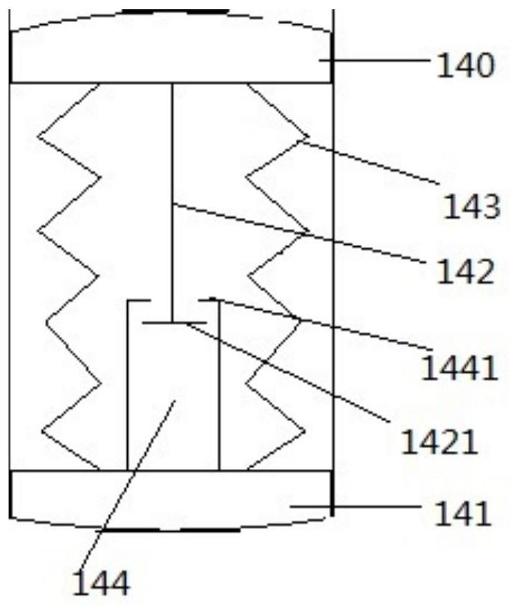
[0034] Embodiment 1 of the present invention provides an electrical connector applied in a vacuum chamber, wherein the vacuum chamber is provided with opposite first terminal posts and second terminal posts, and the electrical connector is arranged on the first terminal posts and the second terminal. figure 1 It shows a schematic structural diagram of an electrical connector used in a vacuum chamber according to Embodiment 1 of the present invention, please refer to figure 1 , the electrical connector includes:
[0035] The first conductive part 140 is arranged opposite to the first terminal, and can be in contact with or away from the first terminal;
[0036] The second conductive part 141 is in contact with the second terminal;
[0037] A stretchable conductive structure located between the first conductive part 140 and the second conductive part 141, the stretchable conductive structure 143, the first conductive part 140 and the second conductive part 141 form a sealed ca...
Embodiment 2
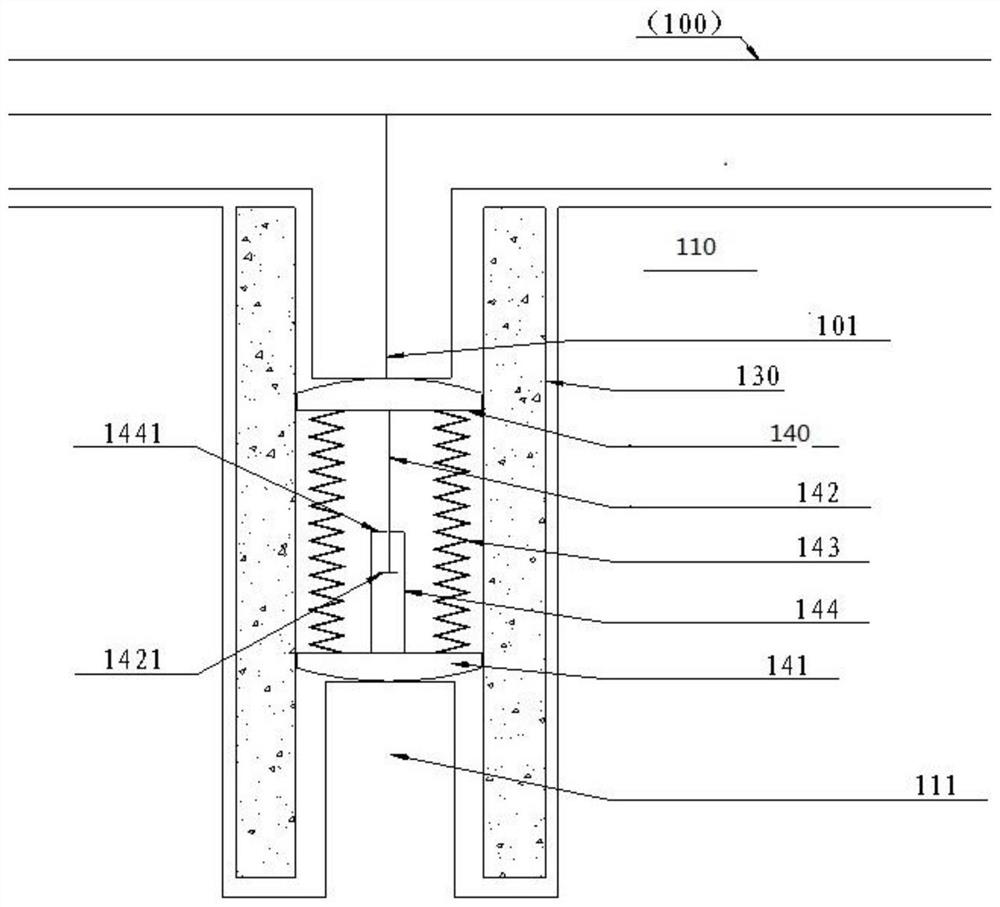
[0049] Embodiment 2 of the present invention provides an electrostatic chuck that can be placed in a vacuum chamber. figure 2 shows a schematic structural diagram of an electrostatic chuck according to Embodiment 2 of the present invention, please refer to figure 2 , the electrostatic chuck includes:
[0050] The metal base 110 , the ceramic body 100 disposed on the metal base 110 , the metal base 110 is provided with a longitudinally arranged accommodation cavity, and the electrical connector of the first embodiment is arranged in the accommodation cavity. The upper end of the accommodating cavity is a first terminal 101 for powering the ceramic body 100 , and the lower end of the accommodating cavity is a second terminal 111 for introducing external electrical signals.
[0051] In this embodiment, the second terminal post 111 is embedded in the metal base 110 and is insulated from the metal base 110 . The second terminal post 111 is used for electrical connection with ext...
PUM
| Property | Measurement | Unit |
|---|---|---|
| thickness | aaaaa | aaaaa |
Abstract
Description
Claims
Application Information

