HJT battery with high photoelectric conversion efficiency and preparation method thereof

A technology for photoelectric conversion efficiency and battery, applied in the field of solar cells, can solve problems such as affecting the quality of the intrinsic layer of amorphous silicon and reducing the open circuit voltage.

Pending Publication Date: 2021-05-07
TONGWEI SOLAR ENERGY CHENGDU CO LID +4
View PDF1 Cites 2 Cited by
  • Summary
  • Abstract
  • Description
  • Claims
  • Application Information

AI Technical Summary

Problems solved by technology

Although this application uses a lightly doped B layer close to the intrinsic layer of amorphous silicon, there will still be a part of B atoms diffused to the intrinsic layer of amorphous silicon, which will affect the film quality of the intrinsic layer of amorphous silicon and affect the open circuit voltage. There is still a certain degree of reduced impact

Method used


Image

  • HJT battery with high photoelectric conversion efficiency and preparation method thereof

Examples


Embodiment 1

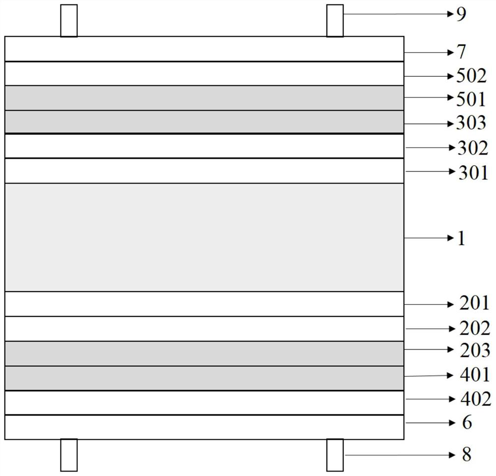
[0038] to combine figure 1 , a kind of high photoelectric conversion efficiency HJT cell of the present embodiment comprises N-type crystalline silicon chip 1, and the front of described N-type crystalline silicon chip 1 is provided with intrinsic amorphous silicon layer 301, SiO 2 Layer 302, C doped SiO 2 layer 303, an amorphous silicon doped N-type layer, a TCO conductive layer 7 and an electrode 9; the back of the N-type crystalline silicon wafer 1 is sequentially provided with an intrinsic amorphous silicon layer 201, SiO 2 Layer 202, C doped SiO 2 layer 203 , amorphous silicon doped P-type layer, TCO conductive layer 6 and electrode 8 . in:

[0039] The thickness of the intrinsic amorphous silicon layer is 3nm.

[0040] The SiO 2 layer and C-doped SiO 2 The thickness of each layer was 1 nm.

[0041] The thickness of the amorphous silicon-doped P-type layer is 10 nm, the thickness of the amorphous silicon-doped N-type layer is 10 nm; the thickness of the TCO conduct...

Embodiment 2

[0044] A HJT battery with high photoelectric conversion efficiency in this embodiment is basically the same as that in Embodiment 1, except that the thickness of the intrinsic amorphous silicon layer is 10 nm.

[0045] The SiO 2 layer and C-doped SiO 2 The thicknesses of the layers were all 5 nm.

[0046] The thickness of the amorphous silicon-doped P-type layer is 30nm, the thickness of the amorphous silicon-doped N-type layer is 30nm; the thickness of the TCO conductive layer is 110nm.

Embodiment 3

[0048] A HJT battery with high photoelectric conversion efficiency in this embodiment is basically the same as that in Embodiment 1, except that the thickness of the intrinsic amorphous silicon layer is 5 nm.

[0049] The SiO 2 Layer thickness 3nm, C-doped SiO 2 The thickness of the layer is 4 nm.

[0050] The thickness of the amorphous silicon-doped P-type layer is 20nm, the thickness of the amorphous silicon-doped N-type layer is 25nm; the thickness of the TCO conductive layer is 100nm.


PUM

PropertyMeasurementUnit
thicknessaaaaaaaaaa
thicknessaaaaaaaaaa
thicknessaaaaaaaaaa

Abstract

The invention discloses an HJT battery with high photoelectric conversion efficiency and a preparation method thereof, and belongs to the technical field of solar cells. The HJT battery comprises an N-type crystal silicon wafer, wherein an intrinsic amorphous silicon layer, a SiO2 layer, a C-doped SiO2 layer, an amorphous silicon doped N-type layer, a TCO conductive layer and an electrode are sequentially arranged on the front surface of the N-type crystal silicon wafer; an intrinsic amorphous silicon layer, a SiO2 layer, a C-doped SiO2 layer, an amorphous silicon doped P-type layer, a TCO conductive layer and an electrode are sequentially arranged on the back surface of the N-type crystal silicon wafer; and the amorphous silicon doped P-type layer comprises a lightly doped B amorphous silicon layer and a heavily doped B amorphous silicon layer. According to the prepared heterojunction solar cell, the photoelectric conversion efficiency can be improved to 24.3% or above, the short-circuit current and the open-circuit voltage are obviously improved, and the photoelectric conversion efficiency of the silicon heterojunction solar cell can be effectively improved.

Description

technical field [0001] The invention relates to the technical field of solar cells, in particular to a HJT cell with high photoelectric conversion efficiency and a preparation method thereof. Background technique [0002] At present, the mainstream battery product in the market is the P-type monocrystalline PERC battery, and the efficiency of the P-type PERC battery has reached the upper limit. However, with the market demand and the continuous development of industry technology, N-type crystalline silicon solar cell technology has received more and more attention in recent years, mainly including passivated emitter back surface fully diffused cells (n-PERT), tunnel oxide Passivated contact cells (TOPCon) and heterojunction cells (HJT), N-type crystalline silicon solar cells have further improved the conversion efficiency of crystalline silicon solar cells. [0003] HJT batteries use cheap amorphous silicon as the emission layer, and the emission layer is doped amorphous si...

Claims


Application Information

Patent Timeline
Patent Type & Authority Applications(China)
IPC IPC(8): H01L31/0747H01L31/0216H01L31/0224H01L31/18H01L31/20
CPCH01L31/02167H01L31/022425H01L31/0747H01L31/1804H01L31/1868H01L31/202Y02P70/50H01L31/208
Inventor 王锦乐肖俊峰
Owner TONGWEI SOLAR ENERGY CHENGDU CO LID
Why Eureka
Try Eureka