

3D storage device and its measurement method, thin film measurement device
A storage device, 3D technology, applied in measurement devices, semiconductor/solid-state device testing/measurement, semiconductor devices, etc., can solve the problems of thin film measurement interference, unreasonable calculation results and actual process results, inability to distinguish, etc. Avoid modeling complex effects
- Summary
- Abstract
- Description
- Claims
- Application Information
AI Technical Summary
Problems solved by technology
Method used
Image

Examples
Embodiment Construction
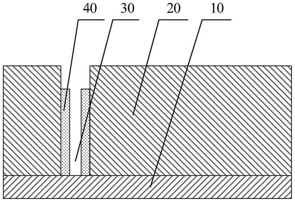
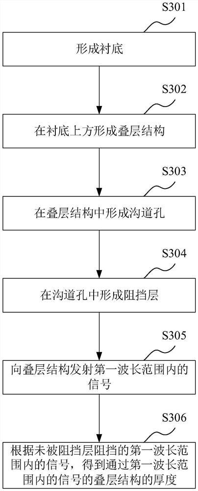
[0039] Various invention will be described in more detail with reference to drawings of the embodiments. In the drawings, the same elements with the same or similar reference numerals. For the sake of clarity, the various parts in the drawings are not drawn. In addition, some well-known portions may not be shown in the figure.
[0040] DETAILED DESCRIPTION OF THE PREFERRED EMBODIMENTS Many of the specific details of the present invention, such as structural, material, size, processing, and techniques of the components are described below, in order to understand the present invention more clearly. However, as will be appreciated by those skilled in the art, the present invention may be implemented without follow these specific details.
[0041] It should be appreciated that, when the structural member is described, when a layer, a region known as another layer, another region when the "on" or "over" may mean directly on another layer above the region, or between it and the other la...
PUM
 Abstract
Description
Claims
Application Information