Method, device and equipment for detecting solder skipping defect of LED, and storage medium

A detection method and defect detection technology, which is applied in the directions of measuring devices, optical testing flaws/defects, image data processing, etc., can solve the problems of reducing the clarity of welding lines and solder joints, visual fatigue of inspectors, false detection, etc.

Active Publication Date: 2021-05-14
高视科技(苏州)股份有限公司
View PDF8 Cites 0 Cited by
  • Summary
  • Abstract
  • Description
  • Claims
  • Application Information

AI Technical Summary

Problems solved by technology

Welding wires are used to connect the positive and negative poles of LED semiconductor chips. Missing soldering will directly lead to unqualified LED products. Therefore, finding a fast and accurate detection method for missing soldering defects in LEDs is important for improving the quality of LED products and reducing production costs. have important meaning
[0003] Most of the traditional welding wire inspections use manual inspection methods. Inspectors need to inspect the welding wires of a large number of products under a microscope for a long time to detect missing welding defects with the naked eye, which will easily cause visual fatigue of the inspectors, resulting in false detections, which is difficult. Ensure the consistency of product quality, especially for LED products with translucent dispensing. Translucent dispensing reduces the clarity of welding lines and solder joints, increasing the difficulty of manual inspection

Method used


Image

  • Method, device and equipment for detecting solder skipping defect of LED, and storage medium
  • Method, device and equipment for detecting solder skipping defect of LED, and storage medium
  • Method, device and equipment for detecting solder skipping defect of LED, and storage medium

Examples


Embodiment 1

[0052] In view of the above problems, the embodiment of the present application provides a detection method for missing soldering defects of LEDs, which can accurately and objectively detect the missing soldering defects of LEDs.

[0053] The technical solutions of the embodiments of the present application are described in detail below with reference to the accompanying drawings.

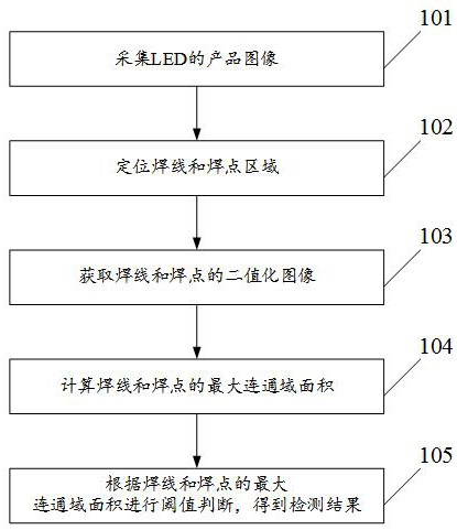
[0054] figure 1 It is a schematic flowchart of a detection method for missing soldering defects of LEDs shown in an embodiment of the present application.

[0055] see figure 1 , the detection method of the missing welding defect of described LED, comprising:

[0056] 101. Collecting LED product images;

[0057] In the embodiment of the present application, the product image of the LED may be a single product image or an entire product image. If the entire product image is collected, the product image is identified and segmented to obtain a single product image, and then step 102 is performed.

...

Embodiment 2

[0098] The embodiment of the present application designs step 102 in the above-mentioned embodiment 1.

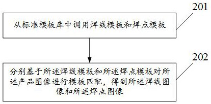
[0099] figure 2 It is a schematic flowchart of a method for positioning welding wires and welding spot regions shown in the embodiment of the present application.

[0100] See details figure 2 , the positioning method of the welding line and the welding point area, comprising:

[0101] 201. Call the welding line template and the welding spot template from the standard template library;

[0102] In the embodiment of the present application, the standard template library may contain various types of LED product templates, and the LED product templates are positioning data obtained by pre-processing according to LED product samples.

[0103] It should be noted that the above description of the standard template library is only an example in the embodiments of the present application, and should not be regarded as a limitation of the present invention.

[0104] 202. Perfo...

Embodiment 3

[0109] In this embodiment of the present application, step 103 in the above-mentioned embodiment 1 is designed.

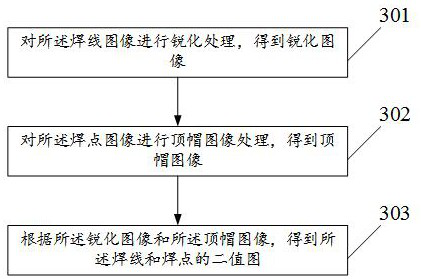
[0110] image 3 It is a schematic flowchart of a method for obtaining a binary image of welding wires and welding spots shown in the embodiment of the present application.

[0111] See details image 3 , the method for obtaining the binary image of the welding wire and the welding spot, comprising:

[0112] 301. Perform sharpening processing on the welding line image to obtain a sharpened image;

[0113] In the embodiment of the present application, the purpose of performing sharpening processing on the welding line image is to highlight the features of the welding line, so as to separate the welding line from the background during subsequent binary image processing.

[0114] It should be noted that there is no strict limitation on the sharpening method used in the embodiment of the present application. In the actual application process, any image sharpening alg...


PUM


Abstract

The invention relates to a method, a device and equipment for detecting a solder skipping defect of an LED, and a storage medium. The method comprises the following steps: collecting an LED product image, processing the product image, and identifying a welding wire area and a welding spot area; carrying out binarization processing on the images of the bonding wires and the welding spots to obtain binary images of the bonding wires and the welding spots; and calculating the areas of the welding wire and the welding spot region based on the welding wire and the welding spot binary image, comparing the areas with a preset area threshold value, and carrying out missing welding defect detection on the LED according to a comparison result. According to the method provided by the invention, the missing welding defect detection of the LED can be simply, accurately and objectively realized.

Description

technical field [0001] The present application relates to the technical field of semiconductors, and in particular to a detection method, device, equipment and storage medium for missing soldering defects of LEDs. Background technique [0002] With the development of LED technology, LED lighting has become more and more widely used in modern technology, and LED technology has gradually occupied an important position in various fields. In the LED production process, the production and packaging process attaches great importance to the yield and quality, so the welding wire defect detection and quality control in the production and packaging process are very important. Welding wires are used to connect the positive and negative poles of LED semiconductor chips. Missing soldering will directly lead to unqualified LED products. Therefore, finding a fast and accurate detection method for missing soldering defects in LEDs is important for improving the quality of LED products and ...

Claims


Application Information

Patent Timeline
Patent Type & Authority Applications(China)
IPC IPC(8): G06T7/00G06T7/11G06T7/136G06T7/187G06T7/62G01N21/88
CPCG01N21/8851G01N2021/8887G06T7/0004G06T2207/30148G06T2207/30152G06T7/11G06T7/136G06T7/187G06T7/62
Inventor 吴晨刚陈健李正大
Owner 高视科技(苏州)股份有限公司
Why Eureka
Try Eureka