Micro OLED display and production method thereof

A production method and a display technology, which are applied in the field of MicroOLED display, can solve the problems of uneven spin coating of organic layers and organic planarization layers and the matching of encapsulation layers, and achieve the effects of avoiding uneven spin coating, high efficiency, and simplified processes

Pending Publication Date: 2021-05-14
ANHUI SEMICON INTEGRATED DISPLAY TECH CO LTD
View PDF0 Cites 1 Cited by
  • Summary
  • Abstract
  • Description
  • Claims
  • Application Information

AI Technical Summary

Problems solved by technology

[0004] In order to solve the above-mentioned technical problems, the present invention provides a Micro OLED display and a production method thereof. The organic layer and the organic planarization layer are prepared by inkjet printing, which can realize the production of the organic planarization layer and the organic layer on demand, and adopt The organic planarization layer is prepared with specific materials to solve the problems of uneven spin coating of the organic layer and the organic planarization layer and the matching between the organic planarization layer and the encapsulation layer, reduce the process and improve the performance of the device

Method used


Image

  • Micro OLED display and production method thereof
  • Micro OLED display and production method thereof
  • Micro OLED display and production method thereof

Examples


Embodiment 1

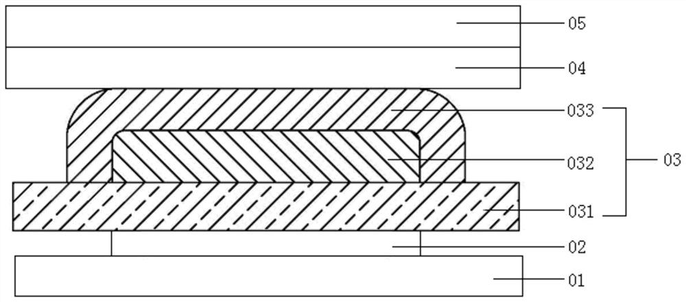
[0035] A production method of a Micro OLED display, comprising the following steps:

[0036] (1) Prepare a CMOS drive circuit on a silicon wafer substrate to obtain a substrate, and prepare an AMOLED light-emitting layer on the substrate according to the pixel arrangement structure;

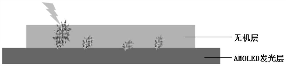
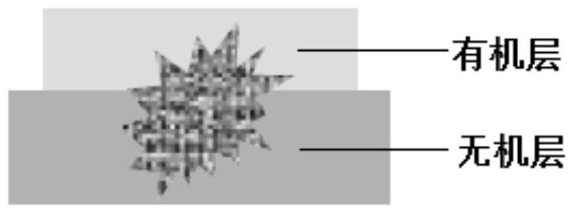
[0037] (2) A first inorganic layer is prepared on the AMOLED light-emitting layer, and an organic layer is prepared by inkjet printing on the first inorganic layer, and the area of ​​the organic layer is smaller than that of the first inorganic layer area, preparing a second inorganic layer on the outer surface of the organic layer to obtain an encapsulation layer positioned on the AMOLED light-emitting layer;

[0038] (3) preparing an organic planarization layer by inkjet printing on the encapsulation layer;

[0039] (4) performing RGB coating on the organic buffer layer to form a color filter layer.

[0040] The material of the organic planarization layer is acrylic resin, and the thickness o...


PUM

PropertyMeasurementUnit
thicknessaaaaaaaaaa
thicknessaaaaaaaaaa
thicknessaaaaaaaaaa

Abstract

The invention discloses a Micro OLED display and a production method thereof. The production method comprises the following steps: producing a CMOS drive circuit on a silicon wafer substrate to obtain a substrate, and producing an AMOLED light-emitting layer on the substrate according to a pixel arrangement structure; preparing an inorganic and organic superposed packaging layer on the AMOLED light emitting layer; preparing an organic planarization layer on the packaging layer in an ink-jet printing mode; and carrying out RGB coating on an organic buffer layer to form a color filter layer. The organic layer and the organic planarization layer are prepared in an ink-jet printing mode, the organic planarization layer and the organic layer can be manufactured as required, the organic planarization layer is prepared from a specific material, the problems that spin coating of the organic layer and the organic planarization layer is not uniform and the organic planarization layer is not matched with the packaging layer are solved, the working procedures are reduced, and the device performance is improved.

Description

technical field [0001] The invention belongs to the technical field of Micro OLED display, and in particular relates to a Micro OLED display and a production method thereof. Background technique [0002] Silicon-based OLED display, as a new display technology combining semiconductor and OLED, will be the main solution for next-generation smart wearable displays such as VR / AR. With the continuous advancement of 5G and AI technology, more and more wearable display products will become more attractive. Silicon-based OLED microdisplay devices have the advantages of high resolution, low power consumption, small size, and light weight, and are widely used in high-resolution near-eye display industries such as AR, VR, wearable devices, industrial security, and medical care. It has become an important point of contention for the new display industry, with huge market potential. The organic light emitting display (Organic Light Emitting Display, OLED) is a new generation of display...

Claims


Application Information

Patent Timeline
Patent Type & Authority Applications(China)
IPC IPC(8): H01L27/32H01L51/52H01L51/56
CPCH10K59/12H10K50/844H10K59/1201H10K71/00
Inventor 程家有李维维曹君赵卓李雪原
Owner ANHUI SEMICON INTEGRATED DISPLAY TECH CO LTD
Why Eureka
Try Eureka