Light emitting diode and preparation method thereof

A technology of light-emitting diodes and second subs, applied in electrical components, circuits, semiconductor devices, etc., can solve the problems of poor heat dissipation, chip burn, uneven chip heat dissipation, etc.

Active Publication Date: 2021-05-14
XIAMEN SANAN OPTOELECTRONICS CO LTD
View PDF13 Cites 0 Cited by
  • Summary
  • Abstract
  • Description
  • Claims
  • Application Information

AI Technical Summary

Problems solved by technology

[0004] In order to solve at least one technical problem in the background technology, the present invention provides a light-emitting diode and a preparation method, which can avoid the phenomenon of uneven heat dissipation of the chip during operation, solve the problem of chip burn caused by poor heat dissipation of the light-emitting diode, and improve the reliability of the chip

Method used


Image

  • Light emitting diode and preparation method thereof
  • Light emitting diode and preparation method thereof
  • Light emitting diode and preparation method thereof

Examples


Embodiment 1

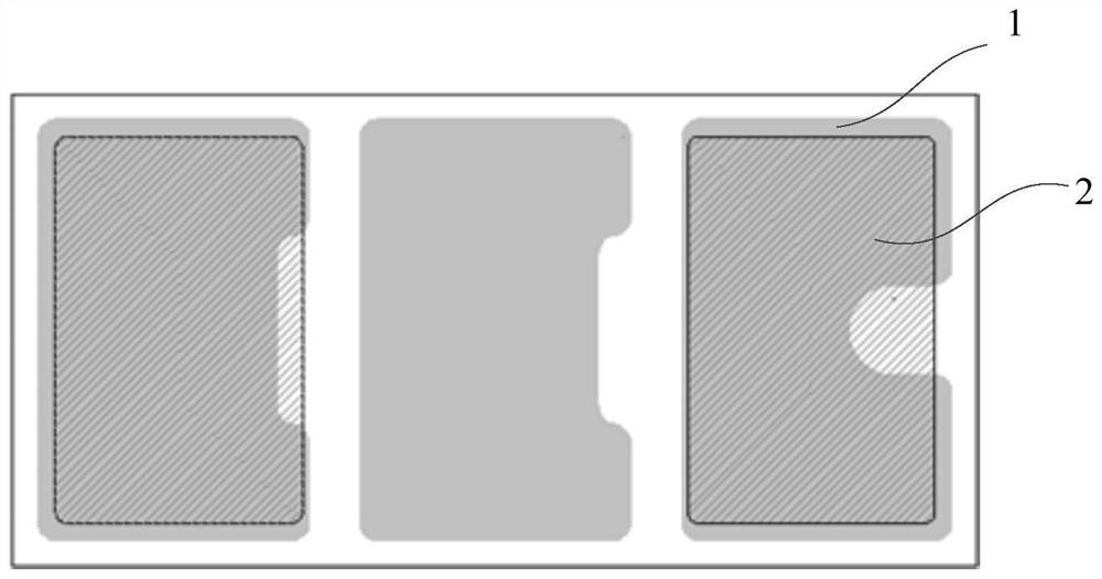
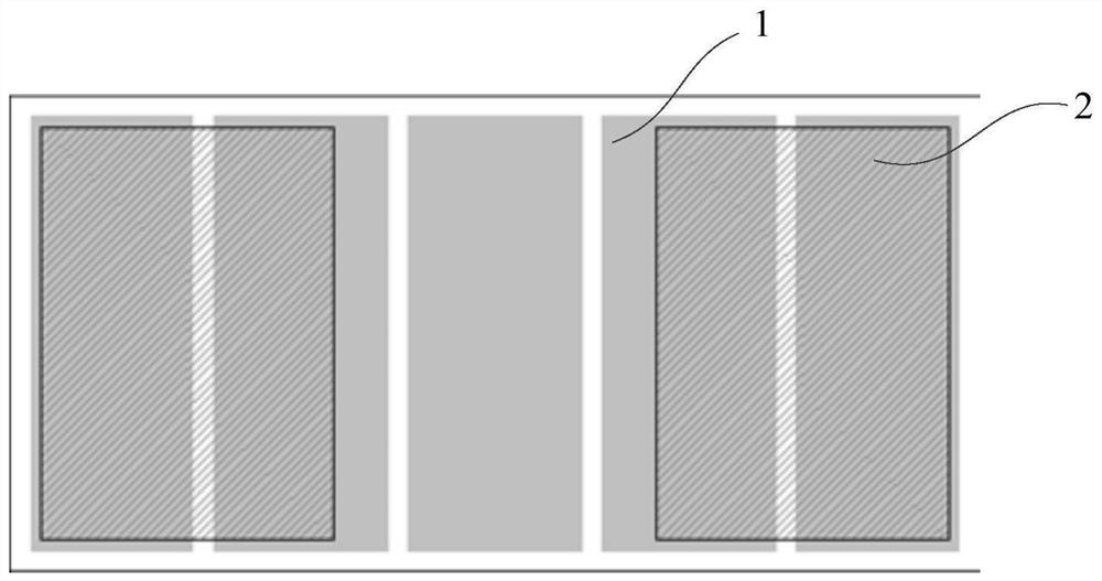
[0064] The light emitting diode provided in this embodiment includes several sub-chips, a first pad, a second pad and other pads, wherein several sub-chips are electrically connected, and adjacent sub-chips are separated by grooves, and at least one sub-chip includes The first semiconductor layer, the active layer and the second semiconductor layer, and the plurality of sub-chips include the first sub-chip, the second sub-chip and at least one other sub-chip except the first sub-chip and the second sub-chip; the first The pad is electrically connected to the second semiconductor layer of the first sub-chip, the second pad is electrically connected to the first semiconductor layer of the second sub-chip, at least one other sub-chip has one other pad, and the other pad is connected to the second semiconductor layer of the second sub-chip. At most one of the first pad or the second pad is electrically connected. Therefore, in the light emitting diode of the present invention, oth...

Embodiment 2

[0079] This embodiment provides a light-emitting diode, which is the same as Embodiment 1 and will not be repeated here. The difference lies in:

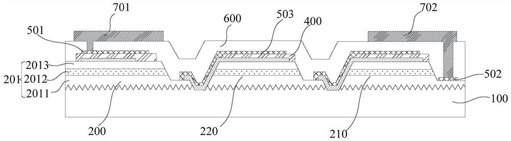
[0080] refer to Figure 7 , the other pads 703 are electrically connected to each other sub-chip through the heat conduction portion 800 disposed in the through hole 603 of the other pad on the reflective layer 600 . Specifically, one end of the heat conduction part 800 is connected to other pads 703 through other heat dissipation vias 603 , and the other end is connected to the epitaxial layer of another sub-chip 220 ; at this time, the other pads 703 and the heat conduction part 800 are both conductive materials. Optionally, a heat dissipation layer 900 is also provided between the heat conduction portion 800 and the epitaxial layers of other chiplets 220 , and the material of the heat dissipation layer 900 is also heat conduction metal. Optionally, the cross-sectional area of ​​the heat dissipation layer 900 is greater than the ...

Embodiment 3

[0083] This embodiment also provides a method for preparing a light-emitting diode, referring to Figure 8 , 4a -4b and 5a-5h; including:

[0084] S101: Obtain several sub-chips that are electrically connected to each other, and adjacent sub-chips are separated by trenches; wherein at least one sub-chip includes at least a first semiconductor layer, an active layer, and a conductive layer opposite to the first semiconductor layer. The epitaxial layer formed by the second semiconductor layer, the several sub-chips include the first sub-chip 200, the second sub-chip 210 and at least one other sub-chip 220 except the first sub-chip 200 and the second sub-chip 210;

[0085] Specifically, a substrate 100 is provided, and the substrate 100 can be one of a sapphire substrate, a silicon carbide substrate, a gallium nitride substrate, a gallium arsenide substrate, a silicon substrate, etc. Forming the epitaxial layer comprising the first semiconductor layer, the active layer and the ...


PUM

PropertyMeasurementUnit
Thicknessaaaaaaaaaa
Thicknessaaaaaaaaaa

Abstract

The invention discloses a light emitting diode and a preparation method thereof. The light emitting diode comprises a plurality of sub-chips which are electrically connected with one another, a first bonding pad, a second bonding pad and other bonding pads, wherein the adjacent sub-chips are spaced by a groove, at least one sub-chip comprises a first semiconductor layer, an active layer and a second semiconductor layer, and the plurality of sub-chips comprise a first sub-chip, a second sub-chip and at least one other sub-chip except the first sub-chip and the second sub-chip. The first bonding pad is electrically connected with the second semiconductor layer of the first sub-chip; the second bonding pad is electrically connected with the first semiconductor layer of the second sub-chip; and at least one other sub-chip is provided with one other bonding pad, and the other bonding pad is electrically connected with at most one of the first bonding pad or the second bonding pad. The phenomenon of non-uniform heat dissipation of the chip can be avoided, the problem of chip burning caused by poor heat dissipation of the light-emitting diode is solved, and the reliability of the chip is improved.

Description

technical field [0001] The invention relates to the technical field of semiconductor devices, in particular to a light emitting diode and a preparation method. Background technique [0002] With the development of LED technology, LEDs directly driven by high voltage have been realized. The efficiency of high-voltage LEDs is better than that of traditional low-voltage LEDs, mainly due to the small current, multi-unit involvement can spread the current evenly, and high-voltage LEDs can realize direct high-voltage drive, thereby saving the cost of LED drive. [0003] The existing high-voltage LED chips have the problems of increased power, difficult heat dissipation and reduced reliability. Usually, in order to ensure the uniformity of the light emission of the high-voltage chip, the chip will be divided into (at least three) sub-chips of equal area by the isolation groove, and each sub-chip is connected in series to realize high-voltage light emission; during this process, th...

Claims


Application Information

Patent Timeline
IPC IPC(8): H01L33/64H01L33/08
CPCH01L33/644H01L33/647H01L33/08
Inventor 刘士伟徐瑾王水杰刘可阙珍妮张中英
Owner XIAMEN SANAN OPTOELECTRONICS CO LTD
Why Eureka
Try Eureka