Packaging structure and packaging method of focal plane detector chip integrated pixel-level lens

A focal plane detector and packaging structure technology, which is applied in the direction of electric solid-state devices, semiconductor devices, sustainable manufacturing/processing, etc., can solve the problem that the window flat film does not have light convergence and collection, and reduces the detection signal-to-noise ratio of the focal plane chip. high cost

Pending Publication Date: 2021-05-18
SUZHOU SUNA PHOTOELECTRIC
View PDF0 Cites 2 Cited by
  • Summary
  • Abstract
  • Description
  • Claims
  • Application Information

AI Technical Summary

Problems solved by technology

[0002] At present, in the industrial fields of visible light, infrared imaging and sensing, focal plane chips of various technologies such as CCD, CMOS, VOx, and InGaAs are widely used to realize imaging of light of specific wavelengths. The packaging methods of these focal plane chips are usually adopted Metal or ceramic shell packaging, the focal plane chip is packaged in a vacuum or nitrogen-filled airtight space to achieve physical pr

Method used


Image

  • Packaging structure and packaging method of focal plane detector chip integrated pixel-level lens
  • Packaging structure and packaging method of focal plane detector chip integrated pixel-level lens
  • Packaging structure and packaging method of focal plane detector chip integrated pixel-level lens

Examples


Embodiment 1

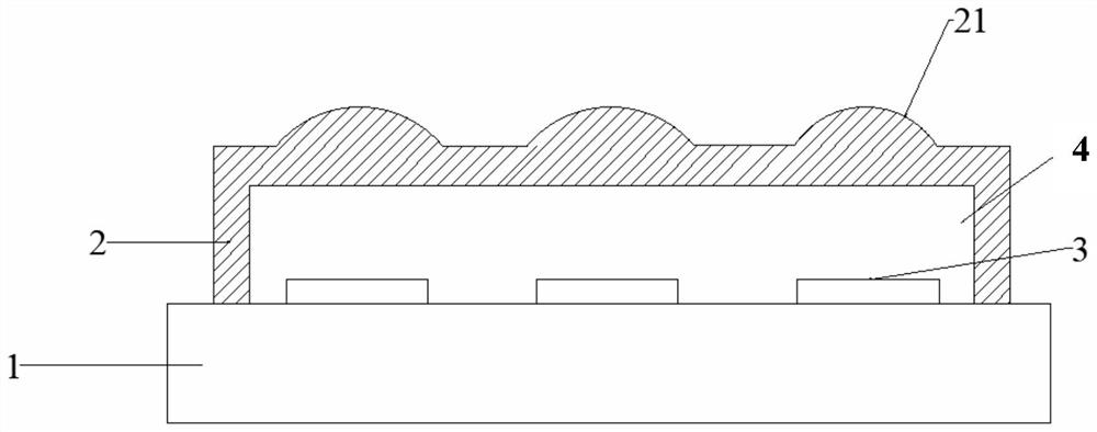
[0049] see figure 1 , a focal plane detector chip integrated pixel-level lens packaging structure, which includes a cooperating package cap 2 and a package base 1, the package cap 2 includes an integrally formed package cap body, a plurality of lenses 21 and an inner concave cavity 4; the plurality of lenses 21 are arranged in an array; the inner concave cavity 4 is used to seal and package a plurality of focal plane detector chips 3; the plurality of focal plane detector chips 3 are all arranged on the packaging base 1 , at the same time, the focus of a lens matched with a focal plane detector chip is distributed on the light-receiving surface of the focal plane detector chip.

Embodiment 2

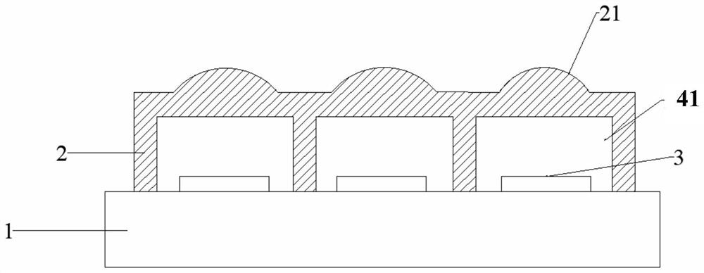
[0051] see figure 2 , a packaging structure of a focal plane detector chip integrated with a pixel-level lens, which includes a package cap 2 and a package base 1 that cooperate with each other, and the package cap 2 includes an integrally formed package cap body, a plurality of lenses 21 and a plurality of internal The concave cavity unit 41; the plurality of lenses 21 are arranged in an array, and are respectively arranged corresponding to the plurality of inner concave cavity units 41; the plurality of inner concave cavity units 41 are respectively used for sealing and packaging a plurality of focal plane detectors chip 3, and isolate the plurality of focal plane detector chips 3 from each other; the plurality of focal plane detector chips 3 are all arranged on the package base 1, and at the same time, a focal plane detector chip matched with a The focus of the lens is distributed on the light-receiving surface of the focal plane detector chip; one of the lenses 21 is inte...

Embodiment 3

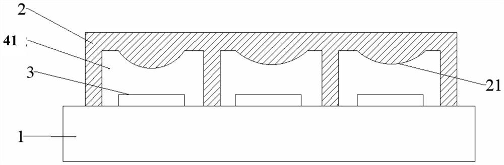
[0066] see image 3 , a packaging structure of a focal plane detector chip integrated with a pixel-level lens, which includes a package cap 2 and a package base 1 that cooperate with each other, and the package cap 2 includes an integrally formed package cap body, a plurality of lenses 21 and a plurality of internal The concave cavity unit 41; the plurality of lenses 21 are arranged in an array, and are respectively arranged corresponding to the plurality of inner concave cavity units 41; the plurality of inner concave cavity units 41 are respectively used for sealing and packaging a plurality of focal plane detectors chip 3, and isolate the plurality of focal plane detector chips 3 from each other; the plurality of focal plane detector chips 3 are all arranged on the package base 1, and at the same time, a focal plane detector chip matched with a The focus of the lens is distributed on the light-receiving surface of the focal plane detector chip; one of the lenses 21 is integ...


PUM


Abstract

The invention discloses a packaging structure and a packaging method for a focal plane detector chip integrated pixel-level lens. The packaging structure comprises a packaging cover cap and a packaging base which are matched with each other, the packaging cover cap comprises a packaging cover cap body, a plurality of lenses and an inner concave cavity which are integrally formed, and the plurality of lenses are arranged in an array; the inner concave cavity is used for sealing and packaging a plurality of focal plane detector chips, the plurality of focal plane detector chips are all arranged on the packaging base, and meanwhile, the focus of a lens matched with one focal plane detector chip is distributed on a light receiving surface of the focal plane detector chip. The size of the packaging structure provided by the invention is greatly reduced; meanwhile, light within the range of the lens can be effectively converged and collected, signals are enhanced, noise is reduced, and the system performance is effectively improved.

Description

technical field [0001] The invention belongs to the technical field of semiconductor manufacturing, and in particular relates to a packaging structure and a packaging method of a focal plane detector chip integrating a pixel-level lens. Background technique [0002] At present, in the industrial fields of visible light, infrared imaging and sensing, focal plane chips of various technologies such as CCD, CMOS, VOx, and InGaAs are widely used to realize imaging of light of specific wavelengths. The packaging methods of these focal plane chips are usually adopted Metal or ceramic shell packaging, the focal plane chip is packaged in a vacuum or nitrogen-filled airtight space to achieve physical protection of the chip and isolation from the outside world. In these packaging methods, anti- The flat window of the anti-film (such as quartz glass) is often larger in size and higher in cost. In addition, since the window plate does not have the function of converging and collecting l...

Claims


Application Information

Patent Timeline
IPC IPC(8): H01L31/0203H01L31/0232H01L25/04H01L31/18
CPCH01L25/042H01L31/0203H01L31/02325H01L31/18Y02P70/50
Inventor 黄寓洋
Owner SUZHOU SUNA PHOTOELECTRIC
Why Eureka
Try Eureka