A 5g communication pcb board

A PCB board and curing board technology, applied in the direction of electrical connection of printed components, reduction of crosstalk/noise/electromagnetic interference (, circuit bendable/stretchable parts, etc., can solve the problem of occupying PCB board work space and complex operation. , The protection effect of the internal layer of the PCB board is poor, etc., to achieve the effect of diversified circuit design and stable signal transmission

A PCB board and curing board technology, applied in the direction of electrical connection of printed components, reduction of crosstalk/noise/electromagnetic interference (, circuit bendable/stretchable parts, etc., can solve the problem of occupying PCB board work space and complex operation. , The protection effect of the internal layer of the PCB board is poor, etc., to achieve the effect of diversified circuit design and stable signal transmission

CN112888145BActive Publication Date: 2022-04-12威利广科技股份有限公司

Image

  • A 5g communication pcb board
  • A 5g communication pcb board
  • A 5g communication pcb board

Examples


Embodiment Construction

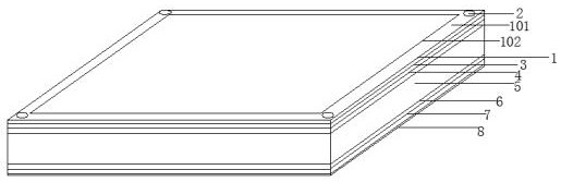
[0027] like Figure 1-6 As shown, a PCB board for 5G communication includes a top layer 1 and a bottom layer 8, the upper end surface of the top layer 1 includes an electrical boundary layer 101 and a component layer 102, the electrical boundary layer 101 is a square layer, and the electrical boundary layer Four installation holes 2 are opened in 101, and the four installation holes 2 are symmetrically distributed on the four corners of the electrical boundary layer 101, and the component layer 102 is located in the middle of the electrical boundary layer 101; the surface of the top layer 1 is set There is a silk screen layer 103, and the surface of the silk screen layer 103 is used for printing component labels and text descriptions, which is convenient for searching components during welding and later circuit maintenance; the silk screen layer 103 covers the upper end surface of the top layer 1; the lower end surface of the top layer 1 A top layer solder resist layer 3 is pr...


PUM


Abstract

The invention discloses a PCB board for 5G communication, comprising a top layer and a bottom layer, the upper end surface of the top layer includes an electrical boundary layer and a component layer, the electrical boundary layer is a square layer, and four Mounting holes, the four mounting holes are symmetrically distributed on the four corners of the electrical boundary layer, the component layer is located in the middle of the electrical boundary layer; the lower end surface of the top layer is provided with a top layer of solder resist, and the top layer of resistance The lower end surface of the solder layer is connected with the first cured plate layer; the upper end surface of the bottom layer is provided with a bottom solder resist layer, and the upper end face of the bottom layer solder resist layer is connected with a second cured plate layer, and the first cured plate layer and An intermediate layer is arranged between the second cured board layers, and a first protective layer and a second protective layer are arranged in the intermediate layer to protect the intermediate layer. A power supply layer is arranged in the intermediate layer, and the two sides of the power supply layer The terminal is provided with a sub butt joint and a female butt joint, which can connect different PCB boards to each other.

Description

technical field [0001] The invention belongs to the technical field of circuit boards, in particular to a PCB board for 5G communication. Background technique [0002] PCB, the Chinese name is printed circuit board, also known as printed circuit board, is an important electronic component, a support for electronic components, and a carrier for electrical connections of electronic components. Because it is made by electronic printing, it is called "printed" circuit board; 5G network is the fifth generation mobile communication network, and its peak theoretical transmission speed can reach 1GB every 8 seconds, which is several times faster than the transmission speed of 4G network. hundred times. For example, a 1G movie can be downloaded within 8 seconds; with the birth of 5G technology, the era of sharing 3D movies, games and ultra-high-definition (UHD) programs with smart terminals is coming to us. The application of 5g will become more and more widespread. [0003] The p...

Claims


Application Information

Patent Timeline
12 Apr 2022
Publication
CN112888145B
IPC
H05K1/02; H05K1/11
CPC
H05K1/0216; H05K1/115; H05K1/0278
Inventors
袁胜巧