Cleaning device for electronic semiconductor machining

A cleaning device and a technology for semiconductors, which are applied in the manufacture of semiconductor/solid-state devices, cleaning methods using tools, cleaning methods using liquids, etc., can solve the damage of fine pattern structure on the surface of semiconductors, the cleaning quality is not high, and the chemical cleaning solution is limited. use, etc.

Inactive Publication Date: 2021-06-04
江西龙芯微科技有限公司
View PDF1 Cites 3 Cited by
  • Summary
  • Abstract
  • Description
  • Claims
  • Application Information

AI Technical Summary

Problems solved by technology

[0008] In order to overcome the defects of the prior art, the technical problem to be solved by the present invention is to propose a cleaning device for electronic semiconductor processing, which solves the problem that the existing cleaning process usually uses liquid chemicals such as acid-base organic matter to soak or rinse the semiconductor, Usually, the removal of particulate pollutants mainly depends on the chemical corrosion of chemical liquid or the physical force introduced in the cleaning process; however, with the

Method used


Image

  • Cleaning device for electronic semiconductor machining
  • Cleaning device for electronic semiconductor machining
  • Cleaning device for electronic semiconductor machining

Examples


Embodiment Construction

[0043] The technical solutions of the present invention will be further described below in conjunction with the accompanying drawings and through specific implementation methods.

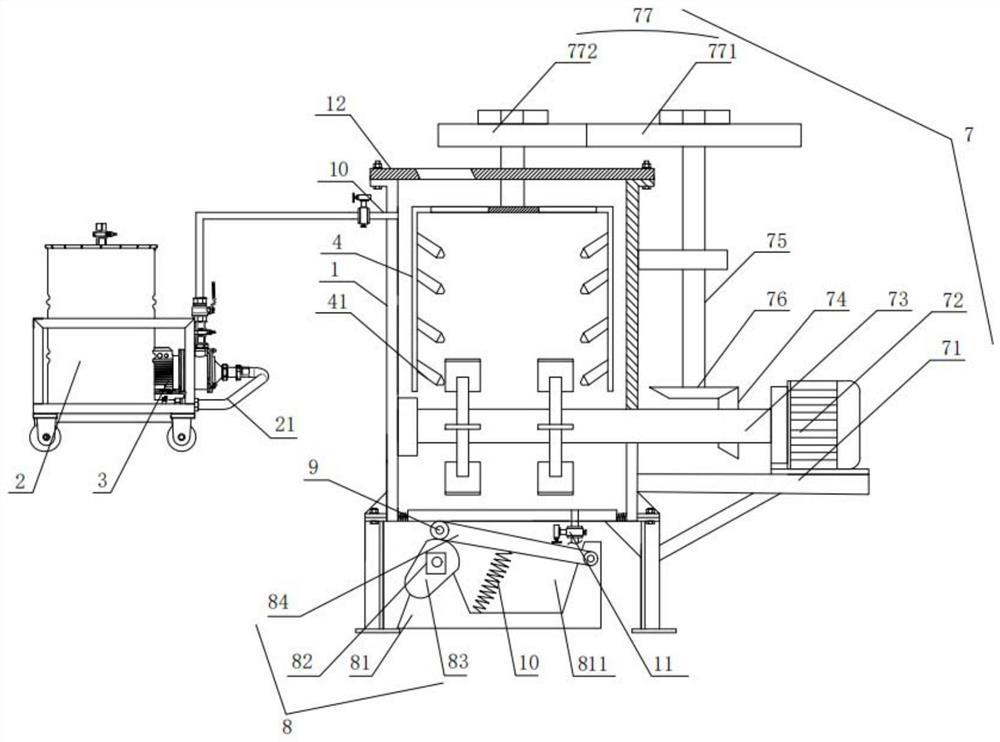
[0044] Figure 1-4 As shown, a cleaning device for electronic semiconductor processing, comprising:

[0045] The megasonic cleaning shell 1, the bottom of the megasonic cleaning shell 1 is provided with an elastic vibrating plate 11 which vibrates periodically; There is a megasonic resonant cavity transducer on the outside;

[0046] The cleaning liquid storage device 2 is used to store the cleaning liquid, and pump the cleaning liquid into the megasonic cleaning shell 1 through the pump body 3;

[0047] The electromagnetic pulse vibrator 4, the electromagnetic pulse vibrator 4 generates pulse vibration in the cleaning liquid, and can be continuously emitted by the electromagnetic pulse source;

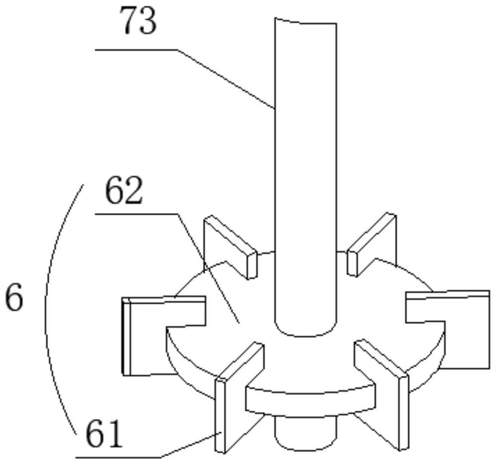
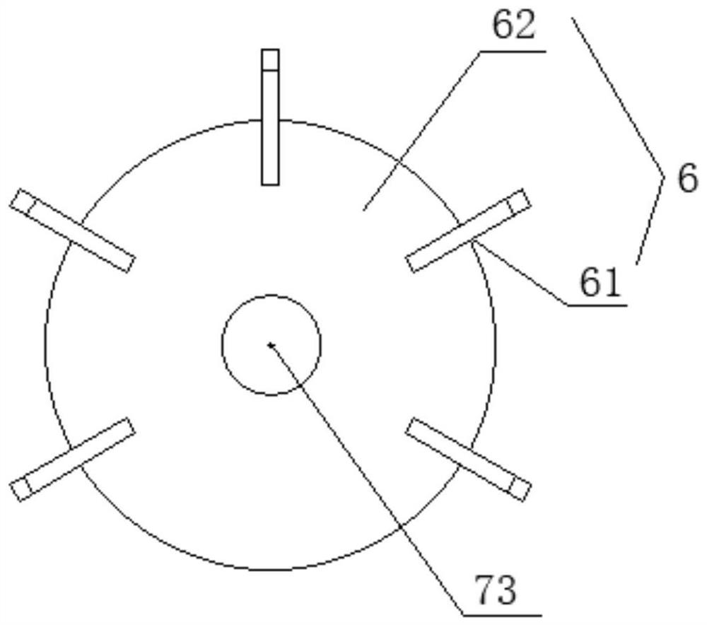
[0048] The cleaning pipeline assembly 5 is distributed in an annular array on the inner wall of the me...


PUM


Abstract

The invention discloses a cleaning device for electronic semiconductor machining. The cleaning device comprises a megasonic cleaning shell, wherein an elastic vibration plate which vibrates periodically is arranged at the bottom of the megasonic cleaning shell; the elastic vibration plate movably covers the bottom of the megasonic cleaning shell; a megasonic resonant cavity transducer is arranged on the outer side of the megasonic cleaning shell; the cleaning device further comprises a cleaning liquid storage device, an electromagnetic pulse vibrator, a cleaning pipeline assembly, a driving part and a vibration assembly, and periodic vibration is generated on the elastic vibration plate; the electromagnetic pulse vibrator and the megasonic resonant cavity transducer are matched to realize high-efficiency cleaning of an electronic semiconductor; and the semiconductor material is flushed more cleanly and cleaned more thoroughly, and the cleaning efficiency and effect are improved.

Description

technical field [0001] The invention relates to the field of cleaning devices, in particular to a cleaning device for electronic semiconductor processing. Background technique [0002] Semiconductors will be polluted by various stains during production, resulting in the failure of semiconductors to achieve the desired effect, especially when cutting and grinding on cast iron grinding discs, resulting in a large damaged layer of silicon wafers after cutting and grinding. The structure makes it difficult to clean, and these are very easy to absorb various impurities, such as particles, organic impurities, inorganic impurities, metal ions, silicon powder dust, etc., especially in the manufacturing process of integrated circuits, particle pollution The control of the amount of species is critical to the final device performance. [0003] In the cleaning process, the important purpose is to control the number of particle pollutants on the surface of the semiconductor and improve...

Claims


Application Information

Patent Timeline
IPC IPC(8): B08B3/12B08B1/00B08B1/02B08B3/02B08B13/00H01L21/67
CPCB08B1/002B08B1/02B08B3/022B08B3/123B08B13/00H01L21/6704H01L21/67046
Inventor 黄晓波
Owner 江西龙芯微科技有限公司
Why Eureka
Try Eureka