A texturing method for pretreating the surface of a single crystal silicon wafer by an electrochemical method
A single crystal silicon wafer, pretreatment technology, applied in chemical instruments and methods, after treatment, single crystal growth, etc., can solve the problems of large consumption of hydrogen peroxide, high requirements for transportation and storage, and increased cost of battery preparation. Achieve the effect of high transportation and storage costs, uniform distribution and simple structure
- Summary
- Abstract
- Description
- Claims
- Application Information
AI Technical Summary
Problems solved by technology
Method used
Image

Examples
Embodiment 1
[0033] The texturing method for electrochemical pretreatment of the surface of a single crystal silicon wafer in this embodiment specifically includes the following steps:
[0034] (1) Immerse the solar monocrystalline silicon wafer in anhydrous ethanol, and ultrasonically clean it at 45-50°C for 5 minutes to remove impurities and organic pollution on the surface of the silicon wafer. Then, the silicon wafer was taken out, washed with deionized water and dried, and then immersed in a 10% NaOH aqueous solution at 85°C for 10 minutes to remove the damaged layer on the surface of the silicon wafer. Then, the silicon wafer was taken out and washed with deionized water. and drying.
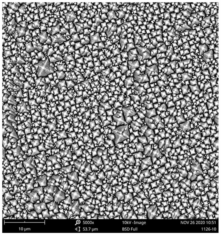
[0035] (2) Electrochemical surface pretreatment is performed on the single crystal silicon wafer treated in the above step (1): the silicon wafer is immersed in K at room temperature of 0.5mol / L 2 SO 4 In the solution, a silicon wafer is used as the anode, and a graphite sheet with an area larger tha...
Embodiment 2
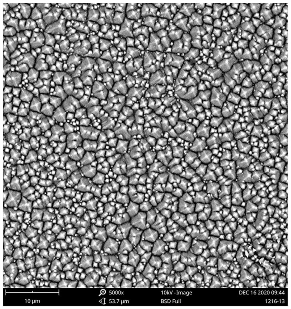
[0038] In this example, the silicon wafer is immersed in a 0.5mol / L NaOH aqueous solution at room temperature, and a DC constant voltage of 2.5V is applied between the anode silicon wafer and the cathode. The other steps are the same as those in Example 1 to obtain a single crystal silicon wafer with a pyramid texture , see figure 2 .
Embodiment 3
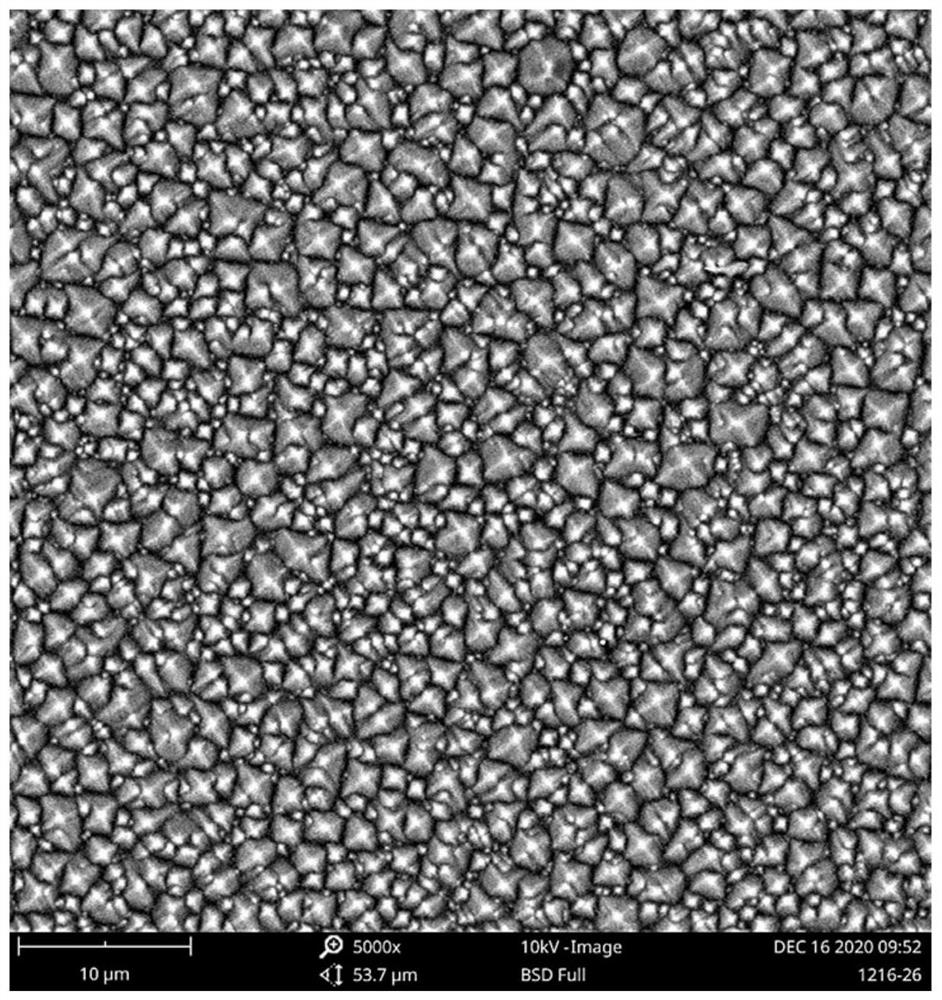
[0040] In this example, the silicon wafer is immersed in a 0.5mol / L hydrochloric acid solution at room temperature, and a DC constant voltage of 2.5V is applied between the anode silicon wafer and the cathode. Other steps are the same as in Example 1 to obtain a single crystal silicon wafer with a pyramid textured structure , see image 3 .
PUM
| Property | Measurement | Unit |
|---|---|---|
| quality score | aaaaa | aaaaa |
| quality score | aaaaa | aaaaa |
| quality score | aaaaa | aaaaa |
Abstract
Description
Claims
Application Information