Power conversion device
A technology for power conversion devices and mounting components, which is applied to output power conversion devices, circuit devices, printed circuit grounding devices, etc. Substrate cost, heat generation suppression, and effects of improved noise resistance
- Summary
- Abstract
- Description
- Claims
- Application Information
AI Technical Summary
Problems solved by technology
Method used
Image
Examples
Embodiment approach 1
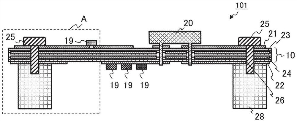
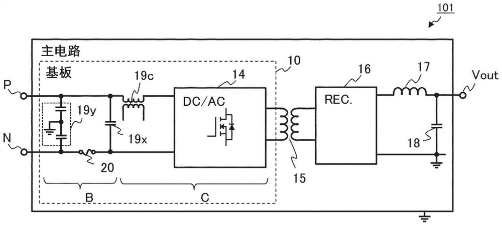
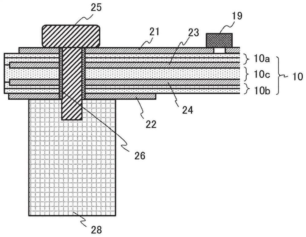
[0026] figure 1 It is a sectional view showing the configuration of the main circuit of the power conversion device according to the first embodiment. figure 2 It is a circuit diagram showing the configuration of the main circuit of the power conversion device. image 3 yes figure 1 A partial enlargement of area A of .
[0027] Such as figure 1 As shown, the main circuit 101 of the power conversion device according to Embodiment 1 is configured to include: a substrate 10; a first wiring layer 21 and a second wiring layer 22 provided on both sides of the substrate 10; The first GND layer 23 and the second GND layer 24 which are arranged on the inner layer part of the substrate 10 under the layer 22 respectively; part 19; a lead insertion part 20 arranged on the surface of the substrate 10 and connected to the first wiring layer 21 and the second wiring layer 22; and a cooler (or case) 28 through which The mounting screw 25 is attached to a through hole 26 as a first throu...
Embodiment approach 2
[0048] In Embodiment 1, a case where wiring layers and GND layers are a four-layer substrate is shown, but in Embodiment 2, a case where wiring layers and GND layers are a six-layer substrate will be described.
[0049] Figure 5 It is a sectional view showing the configuration of the main circuit of the power conversion device according to the second embodiment. Figure 6 yes Figure 5 A partial enlargement of region D of . Such as Figure 5 and Figure 6 As shown in FIG. figure 1 21, Figure 5 , Figure 6 21a) between the first GND layer 23 and the second wiring layer ( figure 1 22, Figure 5 , Figure 6 22a) and the second GND layer 24 are respectively provided with a third wiring layer ( Figure 5 , Figure 6 21b) with the fourth wiring layer ( Figure 5 , Figure 6 22b). Other configurations of the main circuit 102 of the power conversion device according to the second embodiment are the same as those of the main circuit 101 of the power conversion device ac...
PUM
 Abstract
Description
Claims
Application Information


