Supercharge Your Innovation With Domain-Expert AI Agents!

Array substrate

A technology for array substrates and metal layers, which is applied in semiconductor devices, electrical components, circuits, etc., can solve the problems that titanium metal is not resistant to hydrofluoric acid cleaning solution corrosion and affects product quality, so as to ensure electrical conductivity and improve product quality , to avoid the effect of hydrofluoric acid corrosion

Inactive Publication Date: 2021-06-11
WUHAN CHINA STAR OPTOELECTRONICS TECH CO LTD
View PDF5 Cites 2 Cited by
  • Summary
  • Abstract
  • Description
  • Claims
  • Application Information

AI Technical Summary

Problems solved by technology

[0004] Embodiments of the present invention provide an array substrate and a preparation method thereof, to solve the problem of covering the metal material with high temperature resistance and low resistance with titanium metal in the existing array substrate, so as to prevent the metal material from producing hillocks at high temperatures , but titanium metal is not resistant to the corrosion of hydrofluoric acid cleaning solution, which affects the technical problems of product quality

Method used


Image

  • Array substrate
  • Array substrate
  • Array substrate

Examples


Embodiment Construction

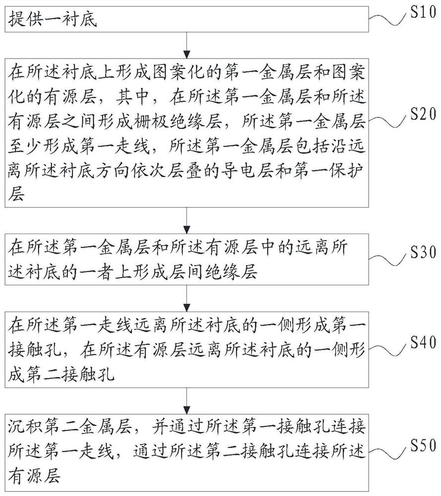
[0027] The following descriptions of the various embodiments refer to the accompanying drawings to illustrate specific embodiments in which the invention may be practiced. The directional terms mentioned in the present invention, such as [top], [bottom], [front], [back], [left], [right], [inside], [outside], [side], etc., are only for reference The orientation of the attached schema. Therefore, the directional terms used are used to illustrate and understand the present invention, but not to limit the present invention. In the figures, structurally similar elements are denoted by the same reference numerals.

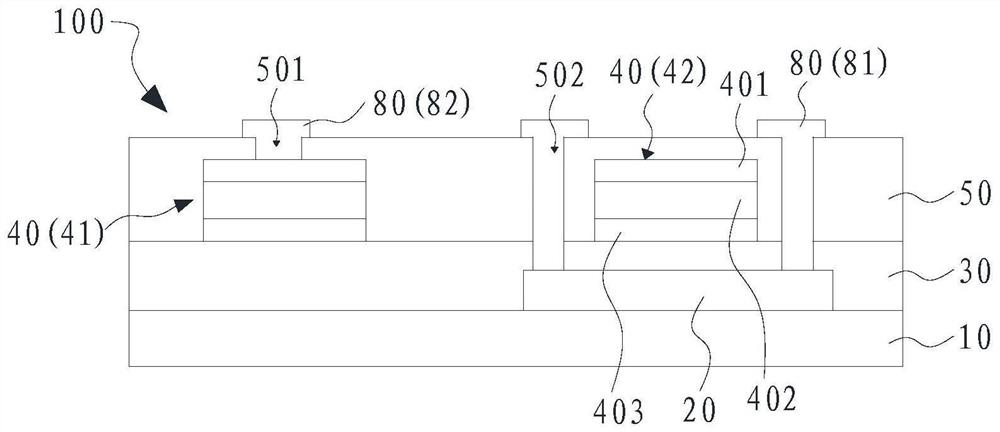
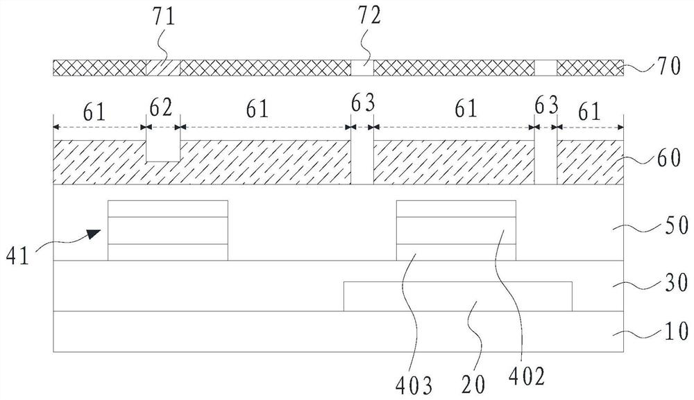
[0028] The present invention aims at the existing array substrate, because the first metal layer tends to produce hillock phenomenon at high temperature, which may lead to the possibility of short-circuiting the adjacent lines or the lines between the upper and lower film layers, thereby affecting the display. Examples to overcome this shortcoming.

[0029] see figur...


PUM

PropertyMeasurementUnit
thicknessaaaaaaaaaa
thicknessaaaaaaaaaa
electrical resistivityaaaaaaaaaa

Abstract

An array substrate comprises a substrate, a first metal layer, an active layer, an interlayer insulating layer and a second metal layer. The first metal layer and the active layer are arranged on the substrate, the first metal layer at least forms a first wire, the interlayer insulating layer is arranged on one of the first metal layer and the active layer far away from the substrate, and the second metal layer is arranged on the interlayer insulating layer. The interlayer insulating layer is provided with a first contact hole, and the second metal layer is connected with the first wire through the first contact hole; wherein the first metal layer comprises a conductive layer and a first protective layer which are sequentially stacked in the direction away from the substrate. The molybdenum material of the first metal layer is replaced by the composite material of the conductive layer and the protective layer which are laminated, so that the conductivity of the first metal layer at high temperature and the function of inhibiting hillock generation are ensured, the protective layer can be prevented from being corroded by hydrofluoric acid in the subsequent process, and the stability of the low-temperature polycrystalline silicon process and the quality of the product are further improved.

Description

technical field [0001] The present invention relates to the field of display technology, in particular to an array substrate. Background technique [0002] The first metal layer wires of LTPS TFT (Low Temperature Poly-Si Thin Film Transistor, low temperature polysilicon thin film transistor) products are limited by the subsequent high-temperature process. At present, most of the mass-produced products in the industry use molybdenum metal, but the impedance of molybdenum metal is relatively high. High-resolution, high-frequency, medium-to-large-size products have a high demand for low-resistance metals. At present, high-temperature-resistant metal materials can be found to replace molybdenum metals to make wires for the first metal layer, such as transfer wires, so that they can be used even at high temperatures. Keeping low resistance, but the first metal layer produced in this way is prone to hillock phenomenon at high temperature, which may cause adjacent wiring or wiring ...

Claims


Application Information

Patent Timeline
Patent Type & Authority Applications(China)
IPC IPC(8): H01L27/12H01L21/77
CPCH01L27/1248H01L27/124H01L27/1259H01L27/1244H01L29/78675H01L29/66757H01L27/1222H01L27/1288
Inventor 马涛许勇温旺林艾飞
Owner WUHAN CHINA STAR OPTOELECTRONICS TECH CO LTD
Features
  • R&D
  • Intellectual Property
  • Life Sciences
  • Materials
  • Tech Scout
  • Unparalleled Data Quality
  • Higher Quality Content
  • 60% Fewer Hallucinations
Learn More