Flexible PCB structure design method based on wet chemical etching joint simulation

A technology for PCB board and structure design, applied in the field of flexible PCB board structure design based on wet chemical etching co-simulation, can solve the problems of high cost, long time, blindness, etc., to improve efficiency and reduce unnecessary losses , cost saving effect

Active Publication Date: 2021-06-15
WUHAN UNIV
View PDF11 Cites 3 Cited by
  • Summary
  • Abstract
  • Description
  • Claims
  • Application Information

AI Technical Summary

Problems solved by technology

[0007] The present invention aims at problems such as time-consuming, high cost, and blindness caused by the trial-and-error method used in the design process of the existing flexible PCB board structure parameters, and proposes a method of etching flexible PCB boards with an etching solution that can reveal controlled flow Mechanism, and the intelligent structural design method of the flexible PCB board with suitable structural parameters based on the mechanism design, so as to achieve the purpose of saving costs, improving efficiency, and scientifically designing structural parameters

Method used


Image

  • Flexible PCB structure design method based on wet chemical etching joint simulation
  • Flexible PCB structure design method based on wet chemical etching joint simulation
  • Flexible PCB structure design method based on wet chemical etching joint simulation

Examples


Embodiment Construction

[0036] The following will clearly and completely describe the technical solutions in the embodiments of the present invention with reference to the accompanying drawings in the embodiments of the present invention. Obviously, the described embodiments are only some of the embodiments of the present invention, not all of them. All other embodiments obtained by persons of ordinary skill in the art based on the embodiments of the present invention belong to the protection scope of the present invention.

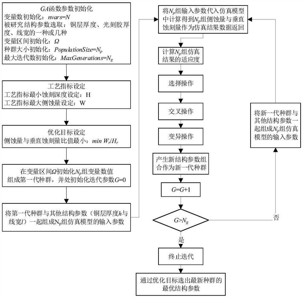
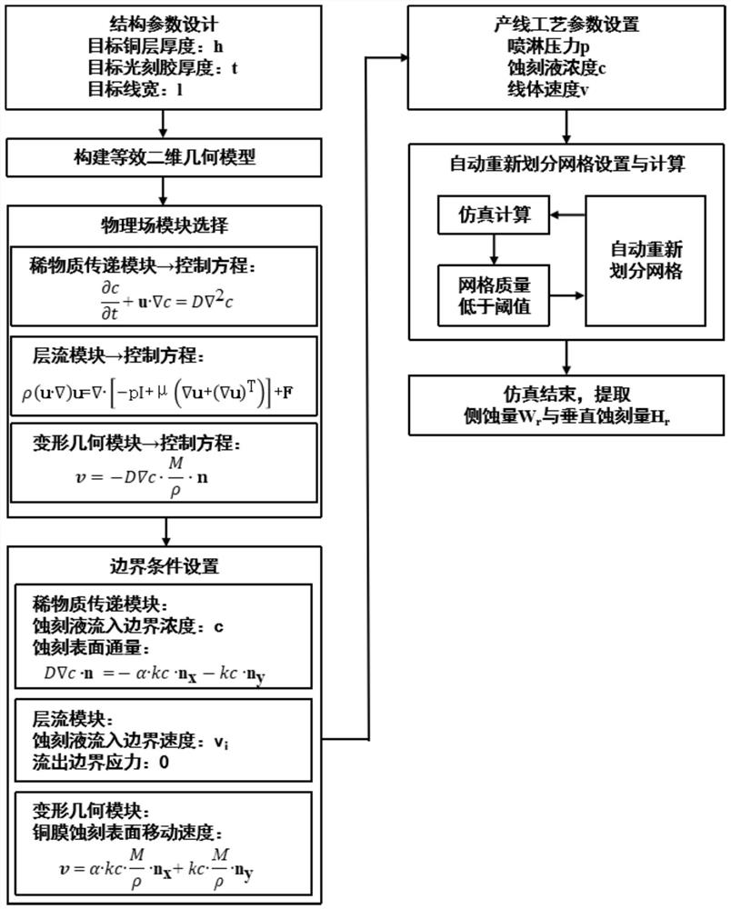
[0037] Such as figure 1 As shown, the present invention provides a kind of multi-physics simulation method, simulates the process of wet chemical etching flexible PCB board, completes the design of structural parameter with simulation method in conjunction with GA algorithm, and this method comprises the following steps:

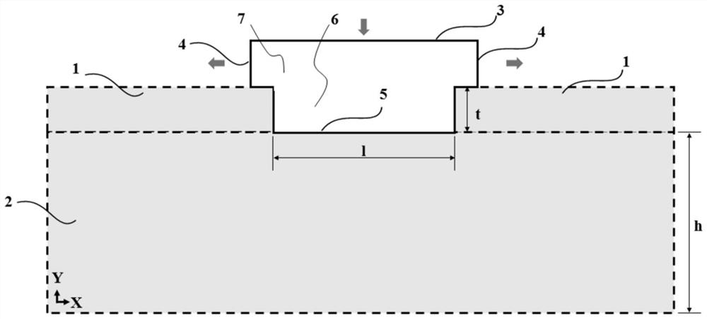
[0038]S1, set the structural parameters of the actual production data according to the needs of the produced PCB products;

[0039] S2. Construct the equival...


PUM


Abstract

The invention discloses a flexible PCB structure design method based on wet chemical etching joint simulation. The method comprises the following steps: firstly, presetting a production parameter data set according to actual production data; then, according to the data set, using multi-physics field finite element simulation software to construct a flexible PCB equivalent two-dimensional geometric model, establishing a multi-physics field simulation model, and completing setting of material attributes, boundary conditions, initial conditions and grids to complete establishment of the simulation model; then calling and iteratively simulating the simulation model by using a model interaction algorithm and a GA according to a preset optimization target and a code parameter set, and curing and reserving optimized structure parameters obtained by simulation for production design. According to the invention, simulation calculation of the structure parameters is carried out through simulation, the structure parameters which are more targeted and meet the actual design requirement can be obtained more intelligently in combination with the GA algorithm, and the method is a scientific design method which can greatly reduce the design cost of a test mode and improve the design time efficiency.

Description

technical field [0001] The technical field of electronic manufacturing of the present invention relates to a simulation optimization-driven electronic manufacturing design technology, in particular to a flexible PCB structure design method based on joint simulation of wet chemical etching. Background technique [0002] Flexible PCB board is a kind of printed circuit board with high quality guarantee and excellent flexibility. It has the characteristics of thin thickness, light weight, good bendability and high wiring density, which can greatly improve space utilization and flexibility. In recent years, flexible PCB boards have been widely used in electronic products such as mobile phones, digital cameras, notebook computers, memory cards, etc., and still have great development potential. [0003] The production process of flexible PCB includes punching, coating, exposure, development, etching, stripping, tinning, automatic optical inspection, ink printing, slitting, circuit...

Claims


Application Information

Patent Timeline
Patent Type & Authority Applications(China)
IPC IPC(8): G06F30/398G06N3/12G06F115/12G06F113/08G06F119/14
CPCG06F30/398G06N3/126G06F2115/12G06F2113/08G06F2119/14
Inventor 李辉申胜男王泽舒盛家正
Owner WUHAN UNIV
Why Eureka
Try Eureka