Method for preparing semiconductor

A technology for semiconductors and substrates, applied in the field of semiconductor structure preparation, can solve the problems of metal layer metal burrs, affecting appearance, affecting product yield, etc.

Active Publication Date: 2021-06-18
度亘激光技术(苏州)有限公司
View PDF4 Cites 1 Cited by
  • Summary
  • Abstract
  • Description
  • Claims
  • Application Information

AI Technical Summary

Problems solved by technology

[0003] In the prior art, after evaporating the metal material, the sidewall of the photoresist column is easily connected with the metal layer. When the photoresist column is removed, the metal adhered

Method used


Image

  • Method for preparing semiconductor
  • Method for preparing semiconductor
  • Method for preparing semiconductor

Examples


Embodiment Construction

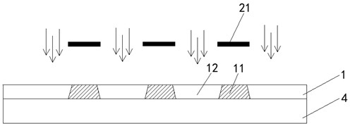
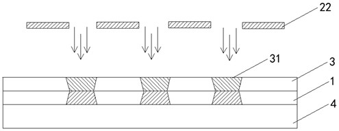
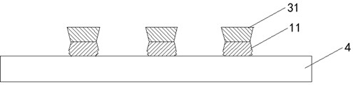
[0032] The technical solutions of the present invention will be described below in conjunction with the drawings, as will be described, as described herein is an embodiment of the invention, not all of the embodiments. Based on the embodiments of the present invention, there are all other embodiments obtained without making creative labor without making creative labor premises.

[0033] In the description of the present invention, it is to be noted that, as shown in terms "center", "upper", "lower", "left", "right", "vertical", "horizontal", "within", " "Wait, the orientation of its indication is based on the orientation or positional relationship shown in the drawings, is meant to facilitate the description of the present invention and simplified description, rather than indicating or implying that the device or component must have a specific orientation. Structure and operation in a specific orientation, it is not understood to limit the limitation of the invention. Further, as ...


PUM


Abstract

The invention provides a method for preparing a semiconductor, and relates to the technical field of semiconductor structure preparation. The method comprises the steps: forming a positive photoresist layer on the upper surface of a substrate; exposing the positive photoresist layer by using the first mask structure, forming a plurality of spaced first inverted trapezoidal structures in an exposure region of the positive photoresist layer, and forming a first regular trapezoidal structure in a non-exposure region between two adjacent first inverted trapezoidal structures; forming a negative photoresist layer above the positive photoresist layer; exposing the negative photoresist layer by using a second mask structure, and forming a second inverted trapezoidal structure in an exposure region of the negative photoresist layer; developing the positive photoresist layer and the negative photoresist layer, and forming a plurality of photoresist columns formed by stacking first positive trapezoidal structures and second inverted trapezoidal structures on the substrate; performing electron beam metal evaporation on one side of the upper surface of the substrate; and performing plasma treatment on the two waists on the same side of the first regular trapezoidal structure along the inclination direction of the two waists of the second inverted trapezoidal structure.

Description

Technical field [0001] The present invention relates to the field of preparation of semiconductor structures, and in particular, to a method of preparing a semiconductor. Background technique [0002] During the preparation of the semiconductor structure, in order to form a spaced metal layer on the substrate, a plurality of intervals of photoresist columns are typically prepared over the substrate, and then precipitate the metal material to the substrate, and the photoresist column is removed. The metal layer is formed. [0003] In the prior art, after the metal material is evaporated, the photoresist column side wall is easy to connect with the metal layer, and when the photoresist column is removed, the metal adhesion to the photoresist column side is also taken away. There is a metal burr on the metal layer, which affects the aesthetics and the product yield. Inventive content [0004] It is an object of the present invention to provide a method of preparing a semiconductor ...

Claims


Application Information

Patent Timeline
IPC IPC(8): H01L21/3205
CPCH01L21/32051
Inventor 浦栋惠利省杨国文
Owner 度亘激光技术(苏州)有限公司
Why Eureka
Try Eureka