Semiconductor structure and forming method thereof

A technology of semiconductor and gate structure, which is applied in the field of semiconductor structure and its formation, can solve the problems of semiconductor device performance to be improved, and achieve the effect of enhancing the ability of the bottom to isolate electron tunneling, improving performance, and increasing the driving current

Pending Publication Date: 2021-06-18
SEMICON MFG INT (SHANGHAI) CORP +1
View PDF0 Cites 0 Cited by
  • Summary
  • Abstract
  • Description
  • Claims
  • Application Information

AI Technical Summary

Problems solved by technology

[0004] However, the performance of semiconductor devices formed by existing technologies needs to be improved

Method used


Image

  • Semiconductor structure and forming method thereof
  • Semiconductor structure and forming method thereof
  • Semiconductor structure and forming method thereof

Examples


Embodiment Construction

[0032] As mentioned in the background, the performance of semiconductor devices formed in the prior art needs to be improved.

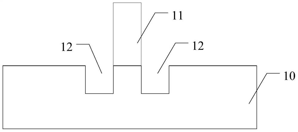
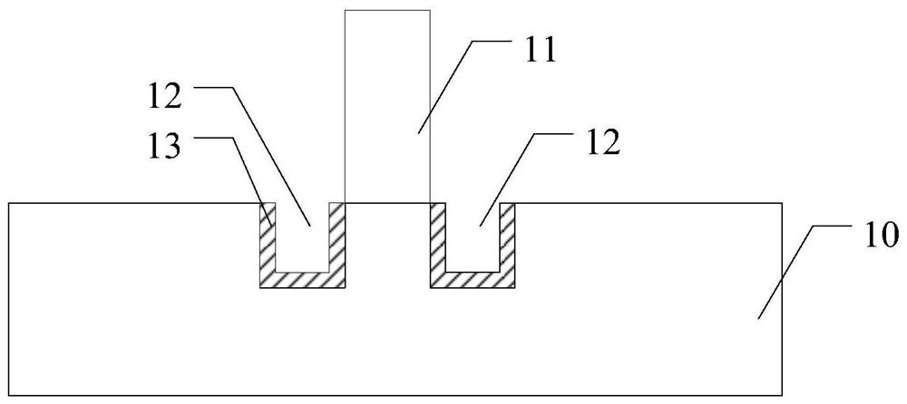
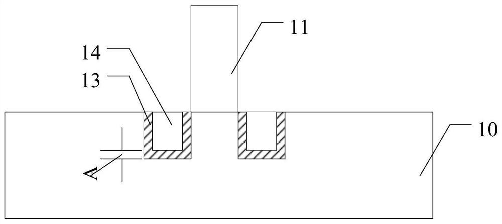
[0033] Figure 1 to Figure 3 It is a schematic cross-sectional structure diagram of the formation process of a semiconductor structure.

[0034] Please refer to figure 1 , providing a substrate 10; forming a gate structure 11 on the surface of the substrate 10; etching part of the substrate 10 on both sides of the gate structure 11 to form an opening 12 in the substrate 10, the The opening 12 is exposed on the surface of the substrate 10 .

[0035] Please refer to figure 2 , forming the first stress layer 13 on the side wall surface and the bottom surface of the opening 12 .

[0036] Please refer to image 3 After the first stress layer 13 is formed, a second stress layer 14 is formed in the opening 12, and the first stress layer 13 and the second stress layer 14 form a source-drain doped layer, thereby forming transistor devices.

[0037] In ...


PUM


Abstract

The invention discloses a semiconductor structure and a forming method thereof. The forming method comprises the following steps: providing a substrate; forming a first gate structure on the surface of the substrate; forming source and drain openings in the substrate at two sides of the first gate structure; forming a first stress layer on the bottom surface and the side wall surface of the source and drain openings; and thinning the side wall of the first stress layer. The semiconductor structure formed by the forming method can improve the performance of a semiconductor device.

Description

technical field [0001] The invention relates to the field of semiconductor manufacturing, in particular to a semiconductor structure and a forming method thereof. Background technique [0002] With the rapid development of integrated circuit manufacturing technology, the size of semiconductor devices in the integrated circuit is continuously reduced, so that the operation speed of the entire integrated circuit will be effectively improved. [0003] In VLSI, stress is usually formed on the transistor to increase the carrier mobility of the transistor to increase the driving current of the transistor. [0004] However, the performance of semiconductor devices formed in the prior art needs to be improved. Contents of the invention [0005] The technical problem solved by the invention is to provide a semiconductor structure and its forming method to improve the performance of semiconductor devices. [0006] In order to solve the above technical problems, the technical solut...

Claims


Application Information

Patent Timeline
Patent Type & Authority Applications(China)
IPC IPC(8): H01L21/336H01L29/78
CPCH01L29/66795H01L29/7848H01L29/785
Inventor 赵猛
Owner SEMICON MFG INT (SHANGHAI) CORP
Why Eureka
Try Eureka