Decorative material, preparation method thereof and electronic equipment
A decorative material and voltage technology, applied in the field of materials, can solve the problems of low bonding force between the coating and the substrate, peeling of the coating, and inability to achieve colorful effects
- Summary
- Abstract
- Description
- Claims
- Application Information
AI Technical Summary
Problems solved by technology
Method used
Image
Examples
preparation example Construction
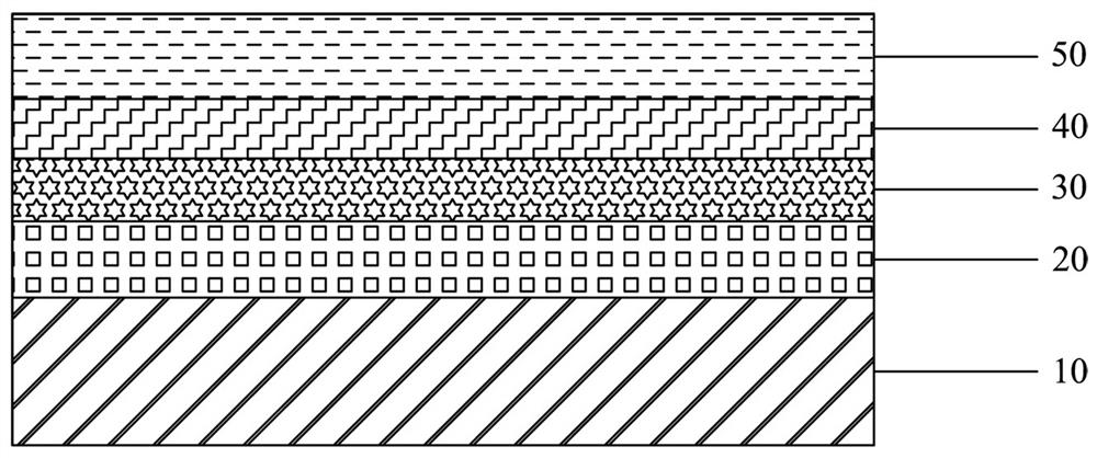
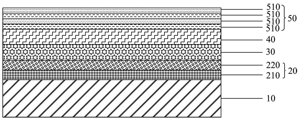
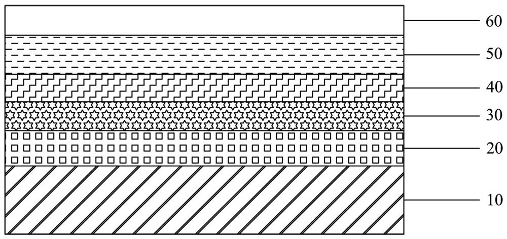
[0034] The second aspect of the present invention provides a method for preparing a decorative material, providing a substrate; forming a transition layer on one side of the substrate; forming a color layer on the side of the transition layer away from the substrate; forming a connecting layer on the side of the color layer away from the transition layer Form the coating layer on the side of the connection layer away from the color layer; Wherein, the coating layer includes multiple sub-coating layers stacked in sequence, and the sub-coating layer close to the connection layer in the multi-layer sub-coating layer is the first sub-coating layer Coating layer, the thermal expansion coefficient of the first sub-coating layer is 3×10 -6 / K-6×10 -6 / K, the thermal expansion coefficient of the connecting layer is 5×10 -6 / K-10×10 -6 / K, and the thermal expansion coefficient of the first sub-coating layer is smaller than the thermal expansion coefficient of the connecting layer. T...
Embodiment 1
[0041] Decorative materials, including: aluminum alloy substrates stacked in sequence, Ti metal transition layer (thickness 30nm), TiSi transition layer (thickness 600nm), TiSiC color layer (thickness 1μm), SiO 2 Connection layer (thickness 30nm), SiO 2 The first sub-coating layer (thickness is 10nm), Ti 3 o 5 Coating layer (thickness 20nm), SiO 2 Coating layer (thickness 20nm), Ti 3 o 5 Coating layer (thickness 40nm), SiO 2 Coating layer (thickness 30nm), Ti 3 o 5 film layer (thickness 20nm) and anti-fingerprint layer, in which SiO 2 The thermal expansion coefficient of the connection layer is 6×10 -6 / K, SiO 2 The thermal expansion coefficient of the first sub-coating layer is 5×10 -6 / K;
[0042] Preparation process of decorative materials:
[0043] (1) Provide aluminum alloy substrate;
[0044] (2) A Ti metal transition layer with a thickness of 30nm is formed on the surface of the aluminum alloy substrate by physical vapor deposition. During the deposition pr...
Embodiment 2
[0051] The structure and preparation process of the decoration material in this embodiment are basically the same as in Example 1, the difference is that the Ti metal transition layer is replaced by a Cr metal transition layer, the TiSi transition layer is replaced by a CrSi transition layer, and the TiSiC color layer is replaced by a CrSiN color layer .
PUM
| Property | Measurement | Unit |
|---|---|---|
| thickness | aaaaa | aaaaa |
| thickness | aaaaa | aaaaa |
| thickness | aaaaa | aaaaa |
Abstract
Description
Claims
Application Information


