Electro-optic crystal thin film for electro-optic modulator, preparation method and electronic components

An electro-optical modulator and electro-optical crystal technology, applied in optical components, optical waveguides and light guides, instruments, etc., can solve problems such as affecting the performance of electronic devices and damage to thin film layers.

Active Publication Date: 2022-05-17
JINAN JINGZHENG ELECTRONICS
View PDF0 Cites 0 Cited by
  • Summary
  • Abstract
  • Description
  • Claims
  • Application Information

AI Technical Summary

Problems solved by technology

[0005] In order to solve the technical problem in the prior art that etching the optical waveguide on the thin film layer will cause certain damage to the thin film layer, thereby affecting the performance of the applied electronic device, this application provides an electro-optical modulator Electro-optic crystal film, preparation method and electronic component

Method used


Image

  • Electro-optic crystal thin film for electro-optic modulator, preparation method and electronic components
  • Electro-optic crystal thin film for electro-optic modulator, preparation method and electronic components
  • Electro-optic crystal thin film for electro-optic modulator, preparation method and electronic components

Examples


Embodiment Construction

[0036] The technical solutions in the embodiments of the present application will be clearly and completely described below with reference to the drawings in the embodiments of the present application. Obviously, the described embodiments are only a part of the embodiments of the present application, but not all of the embodiments. Based on the embodiments in the present application, all other embodiments obtained by those skilled in the art without creative work fall within the protection scope of the present application.

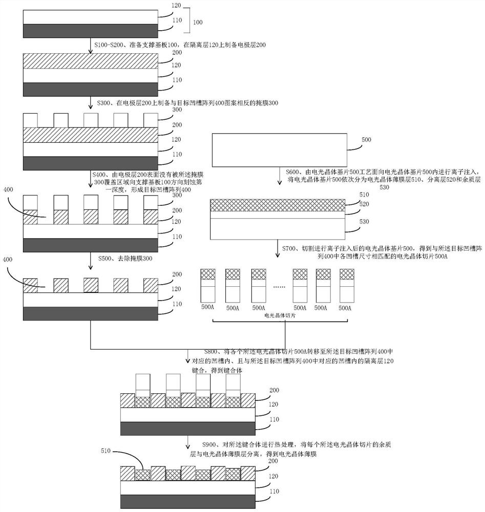
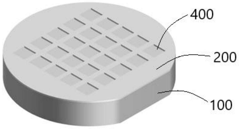
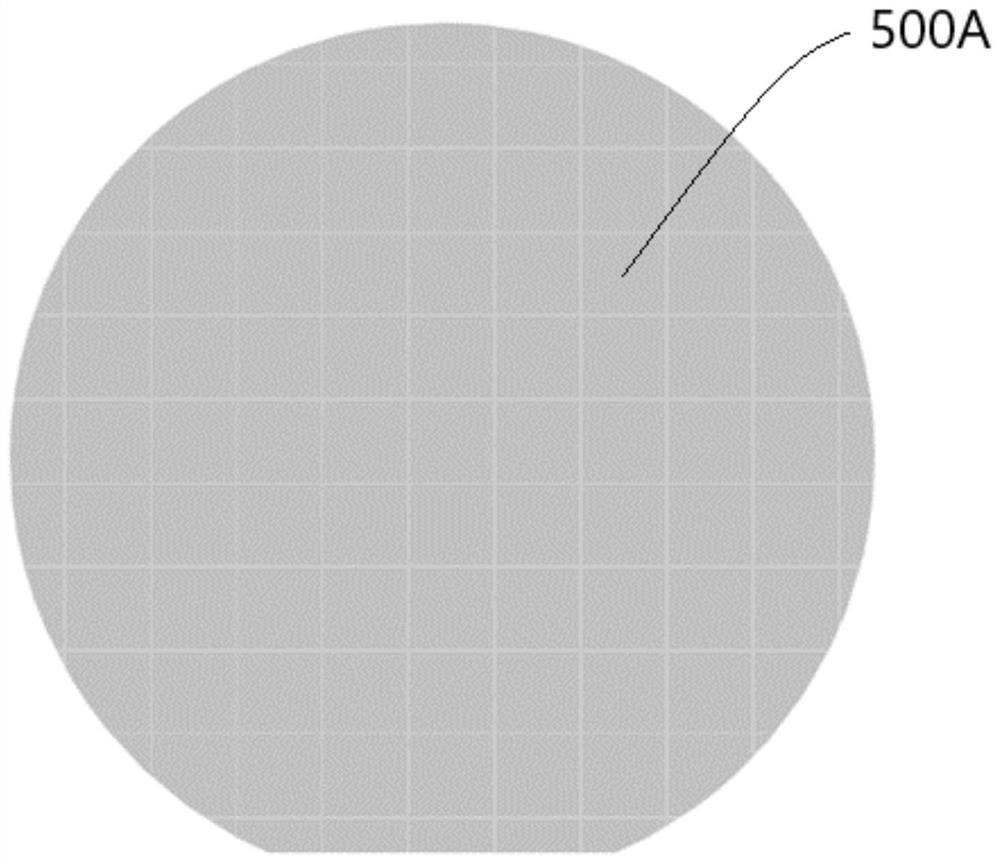
[0037] see figure 1 , the present application provides a method for preparing an electro-optic crystal thin film for an electro-optic modulator, comprising the following steps:

[0038] Step 100 , prepare a support substrate 100 , the support substrate includes a substrate layer 110 and an isolation layer 120 that are sequentially stacked from bottom to top.

[0039] The substrate layer 110 may be a single-layer substrate or a composite substrate, which i...


PUM

PropertyMeasurementUnit
lengthaaaaaaaaaa
lengthaaaaaaaaaa
lengthaaaaaaaaaa

Abstract

The application provides an electro-optic crystal thin film for an electro-optic modulator, a preparation method, and electronic components. A target groove array is prepared on a support substrate laminated with an electrode layer; the electro-optic crystal substrate is ion-implanted and cut into electro-optic Crystal slicing; transferring each electro-optic crystal slice to the corresponding groove in the target groove array, and bonding with the isolation layer in the corresponding groove in the target groove array to obtain a bonded body; performing heat treatment on the bonded body , to obtain electro-optic crystal thin films. This application does not need to etch electro-optic crystal materials with very stable physical and chemical properties such as lithium niobate and lithium tantalate to form optical waveguides, but transfers the cut electro-optic crystal slices to the pre-prepared groove array In the corresponding grooves, the electro-optic crystal film layer remaining in each groove forms an optical waveguide structure, and the optical signal of the optical waveguide is controlled through the grooves formed by the electrodes, thereby realizing the electro-optic modulation function.

Description

technical field [0001] The present application belongs to the technical field of semiconductors, and in particular, relates to an electro-optical crystal film for an electro-optical modulator, a preparation method and an electronic component. Background technique [0002] Electro-optic crystal materials such as lithium niobate or lithium tantalate are widely used in nonlinear optics, ferroelectric, piezoelectric, etc. due to their high Curie temperature, strong spontaneous polarization, high electromechanical coupling coefficient, and excellent electro-optic effect. , electro-optic and other fields, especially in thin-film bulk acoustic wave devices, filters, electro-optic modulators and other fields have received more and more attention and applications. If electro-optical modulators are prepared from electro-optic crystal materials such as lithium niobate or lithium tantalate, the lithium niobate film needs to be further prepared into the required optical waveguide structu...

Claims


Application Information

Patent Timeline
Patent Type & Authority Patents(China)
IPC IPC(8): G02F1/03G02F1/035G02B6/122G02B6/136G02B6/12
CPCG02F1/03G02F1/0305G02F1/0316G02F1/035G02B6/122G02B6/136G02B2006/12142G02B2006/12042G02B2006/12045
Inventor 刘桂银张秀全王金翠连坤
Owner JINAN JINGZHENG ELECTRONICS
Why Eureka
Try Eureka