Electro-optic crystal thin film for electro-optic modulator, preparation method and electronic components

An electro-optical modulator and electro-optical crystal technology, which is applied in the manufacturing of electrical components, optical components, semiconductor/solid-state devices, etc., can solve the problems of thin film layer damage and affecting the performance of electronic devices.

Active Publication Date: 2022-05-10
JINAN JINGZHENG ELECTRONICS
View PDF19 Cites 0 Cited by
  • Summary
  • Abstract
  • Description
  • Claims
  • Application Information

AI Technical Summary

Problems solved by technology

[0005] In order to solve the technical problem in the prior art that etching the optical waveguide on the thin film layer will cause certain damage to the thin film layer, thereby affecting the performance of the applied electronic device, this application provides an electro-optical modulator Electro-optic crystal film, preparation method and electronic component

Method used


Image

  • Electro-optic crystal thin film for electro-optic modulator, preparation method and electronic components
  • Electro-optic crystal thin film for electro-optic modulator, preparation method and electronic components
  • Electro-optic crystal thin film for electro-optic modulator, preparation method and electronic components

Examples


Embodiment Construction

[0034] The following will clearly and completely describe the technical solutions in the embodiments of the application with reference to the drawings in the embodiments of the application. Apparently, the described embodiments are only some of the embodiments of the application, not all of them. Based on the embodiments in this application, all other embodiments obtained by those skilled in the art without making creative efforts belong to the scope of protection of this application.

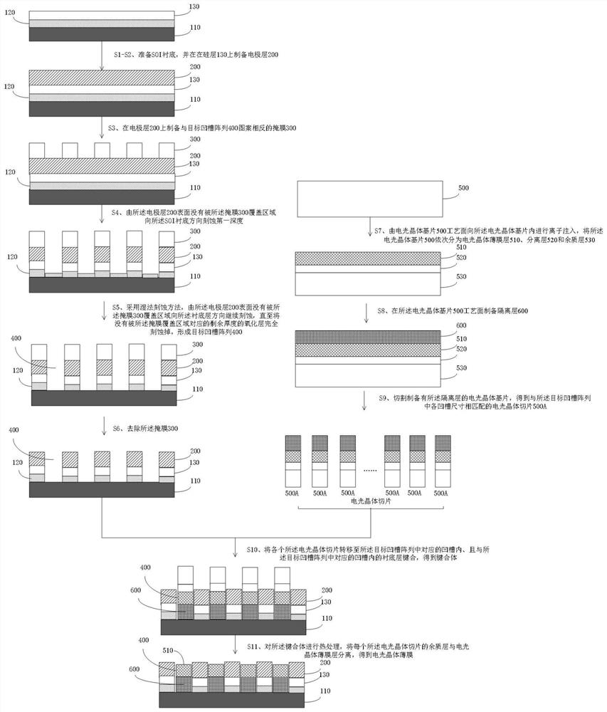
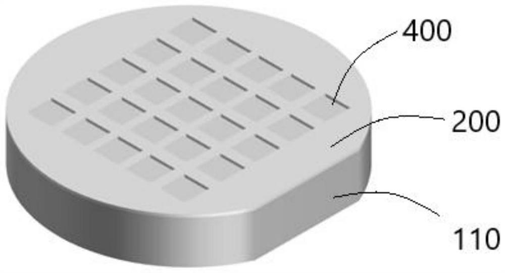
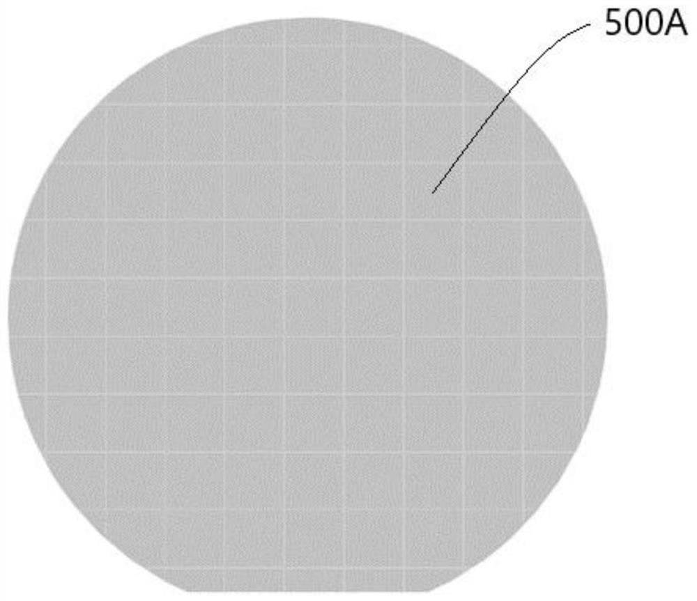
[0035] see figure 1 , the application provides a method for preparing an electro-optic crystal film for an electro-optic modulator, comprising the following steps:

[0036] Step 1. Prepare an SOI substrate, which includes a substrate layer 110 , an oxide layer 120 and a silicon layer 130 sequentially stacked from bottom to top.

[0037] SOI (Silicon-On-Insulator, silicon on insulating substrate), introduces a buried oxide layer between the top silicon layer and the substrate layer. By forming...


PUM

PropertyMeasurementUnit
lengthaaaaaaaaaa
lengthaaaaaaaaaa
lengthaaaaaaaaaa

Abstract

The application discloses an electro-optic crystal thin film for an electro-optic modulator, a preparation method and electronic components. A target groove array is prepared on an SOI substrate laminated with an electrode layer; the electro-optic crystal substrate is ion-implanted and cut into Electro-optic crystal slicing; transferring each electro-optic crystal slice to the corresponding groove in the target groove array, and bonding with the substrate layer in the corresponding groove in the target groove array to obtain a bonded body; performing the bonding on the bonded body Heat treatment to obtain electro-optic crystal thin film. In this application, the electro-optic crystal thin film layer retained in each groove forms an optical waveguide structure, and the optical signal of the optical waveguide is controlled through the grooves formed by the electrodes, thereby realizing the electro-optical modulation function. At the same time, this application uses SOI as the substrate, and uses the characteristics of the smooth surface between the layers of the SOI substrate itself, and combines the wet etching method to etch away the oxide layer in the corresponding area, so as to obtain the substrate layer that meets the needs of direct bonding. surface.

Description

technical field [0001] The application belongs to the technical field of semiconductors, and in particular relates to an electro-optic crystal thin film used for an electro-optic modulator, a preparation method and electronic components. Background technique [0002] Electro-optic crystal materials such as lithium niobate or lithium tantalate are widely used in nonlinear optics, ferroelectricity, and piezoelectricity due to their advantages such as high Curie temperature, strong spontaneous polarization, high electromechanical coupling coefficient, and excellent electro-optic effect. , electro-optic and other fields, especially in the fields of thin-film bulk acoustic wave devices, filters, electro-optic modulators, etc., have received more and more attention and applications. If electro-optic modulators are prepared using electro-optic crystal materials such as lithium niobate or lithium tantalate, it is necessary to further prepare the lithium niobate film into the require...

Claims


Application Information

Patent Timeline
Patent Type & Authority Patents(China)
IPC IPC(8): G02F1/03G02F1/035G02B6/122G02B6/136G02B6/12H01L21/304
CPCG02F1/03G02F1/0305G02F1/0316G02F1/035G02B6/122G02B6/136H01L21/3043G02B2006/12142G02B2006/12042G02B2006/12045
Inventor 刘桂银张秀全王金翠连坤
Owner JINAN JINGZHENG ELECTRONICS
Why Eureka
Try Eureka