Electro-optic crystal thin film for electro-optic modulator, preparation method and electronic components

An electro-optic modulator and electro-optic crystal technology, which is applied in optical components, optical waveguides, instruments, etc., can solve problems affecting the performance of electronic devices and damage to film layers, and achieve the goal of preventing optical signals from leaking to the substrate layer and having a small thickness Effect

Active Publication Date: 2022-05-31
JINAN JINGZHENG ELECTRONICS
View PDF6 Cites 0 Cited by
  • Summary
  • Abstract
  • Description
  • Claims
  • Application Information

AI Technical Summary

Problems solved by technology

[0005] In order to solve the technical problem in the prior art that etching the optical waveguide on the thin film layer will cause certain damage to the thin film layer, thereby affecting the performance of the applied electronic device, this application provides an electro-optical modulator Electro-optic crystal film, preparation method and electronic component

Method used


Image

  • Electro-optic crystal thin film for electro-optic modulator, preparation method and electronic components
  • Electro-optic crystal thin film for electro-optic modulator, preparation method and electronic components
  • Electro-optic crystal thin film for electro-optic modulator, preparation method and electronic components

Examples


Embodiment Construction

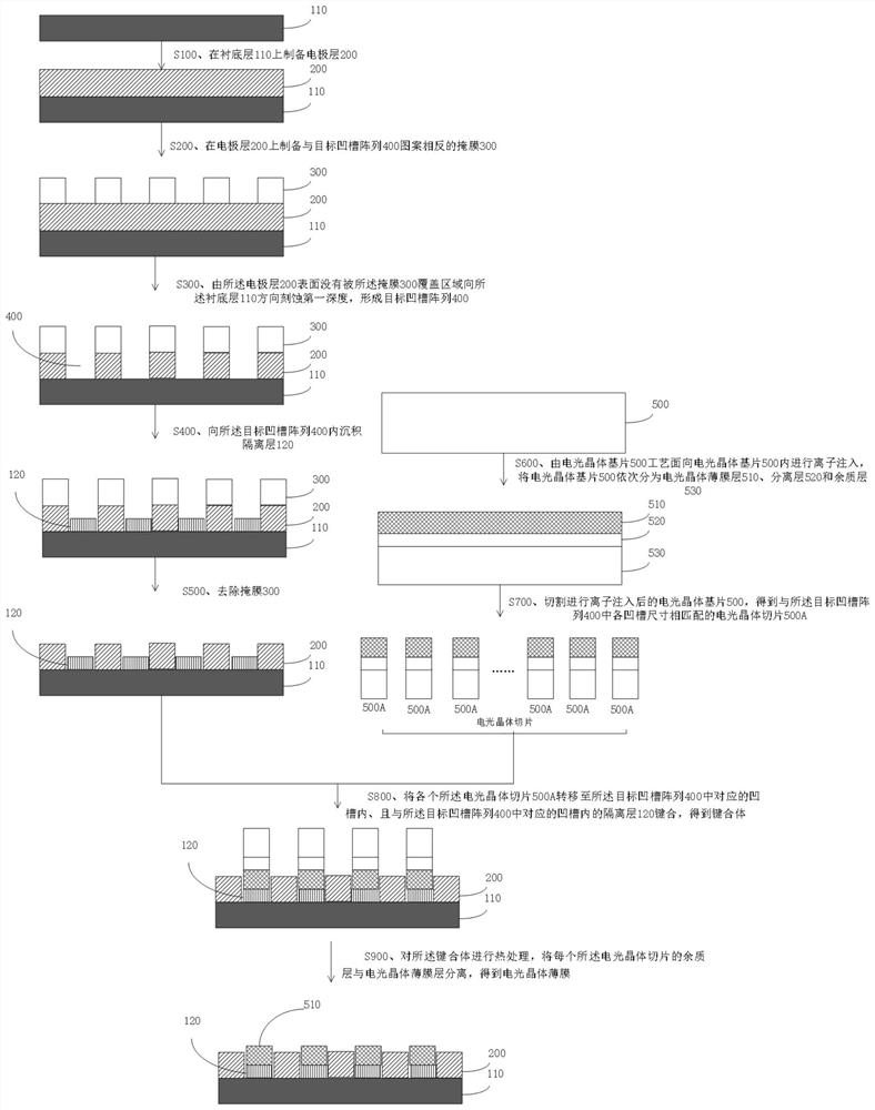
[0036] In step 100, an electrode layer 200 is prepared on the substrate layer 110.

[0037] The substrate layer 110 may be a single-layer substrate or a composite substrate, which is not limited in this application. Substrate layer of this application

[0038] The electrode layer 200 should be selected from metal materials with good electrical conductivity, such as copper (Cu), gold (Au), titanium (Ti), platinum

[0040] Further, the thickness of the Au layer is greater than the thickness of the Cr layer. Since the Au layer mainly functions as an electrode

[0041] The present application does not limit the method for preparing the electrode layer 200, for example: using a magnetron sputtering method, on a silicon wafer

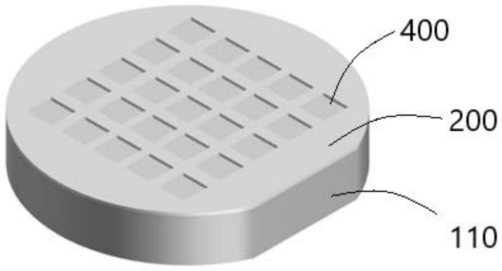
[0042] In step 200, a mask 300 having a pattern opposite to that of the target groove array 400 is prepared on the electrode layer 200.

[0045] The embodiment of the present application does not limit the method for preparing the mask 300 on the electrode layer ...


PUM

PropertyMeasurementUnit
lengthaaaaaaaaaa
lengthaaaaaaaaaa
lengthaaaaaaaaaa

Abstract

The electro-optic crystal thin film for electro-optic modulator, preparation method and electronic components provided by this application, prepare target groove array on the substrate layer laminated with electrode layer; perform ion implantation on electro-optic crystal substrate, and cut into electro-optic crystal Slicing; transferring each electro-optic crystal slice to the corresponding groove in the target groove array, and bonding with the isolation layer in the corresponding groove in the target groove array to obtain a bonded body; performing heat treatment on the bonded body, Electro-optic crystal thin films were obtained. In this application, the electro-optic crystal thin film layer retained in each groove forms an optical waveguide structure, and the optical signal of the optical waveguide is controlled through the grooves formed by the electrodes, thereby realizing the electro-optical modulation function. At the same time, this application only forms the isolation layer on the etched area of ​​the substrate layer, instead of sandwiching an isolation layer between the substrate layer and the electrode layer, so as to prevent the optical signal from leaking to the substrate layer and ensure the overall The thickness of the structure is small.

Description

Electro-optic crystal film for electro-optic modulator, preparation method and electronic component technical field The application belongs to semiconductor technical field, relate in particular to a kind of electro-optical crystal film for electro-optical modulator, system Preparation method and electronic components. Background technique Electro-optic crystal materials such as lithium niobate or lithium tantalate have high Curie temperature, strong spontaneous polarization, and electromechanical coupling system. It is widely used in nonlinear optics, ferroelectric, piezoelectric, electro-optic and other fields, especially It has received more and more attention and applications in the fields of thin-film bulk acoustic wave devices, filters, electro-optic modulators, etc. if using To prepare electro-optic modulators from electro-optic crystal materials such as lithium niobate or lithium tantalate, it is necessary to further prepare the lithium niobate film into the...

Claims


Application Information

Patent Timeline
Patent Type & Authority Patents(China)
IPC IPC(8): G02F1/03G02F1/035G02B6/122G02B6/136G02B6/12
CPCG02F1/03G02F1/0305G02F1/0316G02F1/035G02B6/122G02B6/136G02B2006/12142G02B2006/12042G02B2006/12045
Inventor 刘桂银张秀全王金翠连坤
Owner JINAN JINGZHENG ELECTRONICS
Why Eureka
Try Eureka