
A radiation-resistant high-voltage esd semiconductor device

A semiconductor and anti-radiation technology, applied in the direction of semiconductor devices, electric solid devices, transistors, etc., can solve the problems of high working voltage, ESD damage of circuits and devices, etc., and achieve the effect of increasing the maintenance voltage, avoiding ESD damage, and increasing the opening threshold

Active Publication Date: 2022-08-02
58TH RES INST OF CETC
View PDF3 Cites 0 Cited by
  • Summary
  • Abstract
  • Description
  • Claims
  • Application Information

AI Technical Summary

Problems solved by technology

Especially for radiation-resistant high-voltage integrated circuits, circuits and devices are more prone to ESD damage due to high operating voltages

Method used


Image

  • A radiation-resistant high-voltage esd semiconductor device
  • A radiation-resistant high-voltage esd semiconductor device
  • A radiation-resistant high-voltage esd semiconductor device

Examples


Embodiment 1

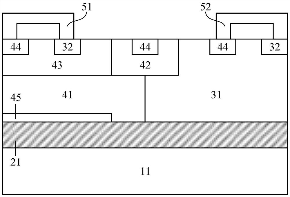
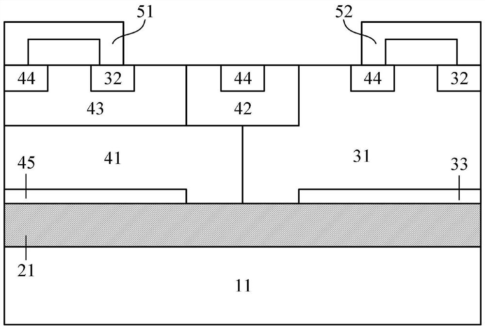
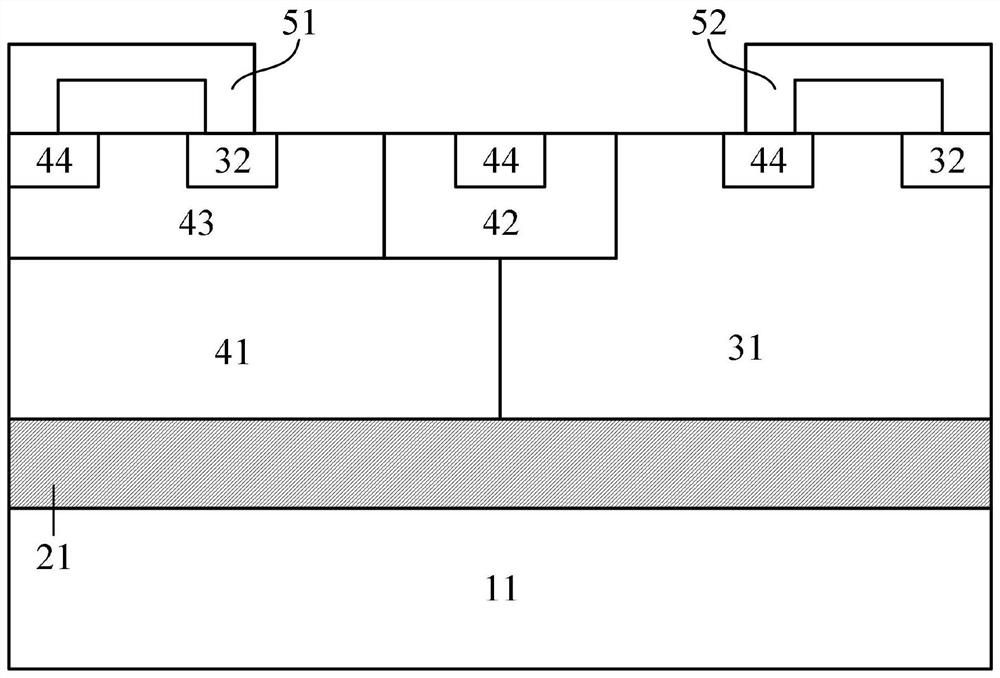
[0019] The present invention provides a radiation-resistant high-voltage ESD semiconductor device, the structure of which is as follows: figure 1 As shown, it includes a P-type substrate 11, a buried oxide layer 21, an N-type well region 31, a P-type well region 41, a P-type drift region 42, a P-type first heavily doped region 43, and a P-type second heavily doped region. Region 44, P-type buried layer 45, N-type heavily doped region 32, anode metal electrode 51, cathode metal electrode 52; N-type well region 31 and P-type well region 41 are arranged on the buried oxide layer 21, P-type first The heavily doped region 43 is located on the top of the P-type well region 41, and the P-type buried layer 45 is arranged on the bottom of the P-type well region 41; the P-type drift region 42 is located on the top of the N-type well region 31 and the P-type well region 41 at the same time, and At the same time, it is in contact with the N-type well region 31 and the P-type well region 4...


PUM


Abstract

The invention discloses a radiation-resistant high-voltage ESD semiconductor device, which belongs to the technical field of semiconductors. In the present invention, a P-type drift region is introduced on the upper surfaces of the P-type well region and the N-type well region, and the withstand voltage between the P-type drift region and the N-type well region determines the trigger voltage of the ESD device, and the withstand voltage is related to the PMOS device's trigger voltage. The breakdown structure is consistent, so the internal devices will be protected during circuit operation to avoid ESD damage. The P-type first heavily doped region is introduced on the surface of the P-type well region, which increases the base region concentration of the parasitic triode NPN device, reduces the base region transport coefficient, and avoids single-particle radiation. The device's resistance to single-event latch-up also improves the device's sustain voltage. The P-type buried layer above the buried oxide layer reduces the parallel resistance of the emitter junction of the parasitic NPN triode, improves the turn-on threshold of the parasitic NPN triode, and further improves the anti-single event latch-up capability of the ESD device.

Description

technical field [0001] The present invention relates to the technical field of semiconductors, in particular to a radiation-resistant high-voltage ESD semiconductor device. Background technique [0002] The phenomenon of electrostatic discharge widely exists in nature, and it is one of the important reasons for the failure of integrated circuit products. Integrated circuit products are easily affected by electrostatic discharge during their manufacturing and assembly processes, resulting in reduced product reliability or even damage. Electro-Static Discharge (ESD) design is an important part of integrated circuit reliability design, and with the development of integrated circuit technology, more challenges will be faced. The research on electrostatic discharge protection devices and circuits with high reliability and strong electrostatic protection performance plays an important role in improving the yield and reliability of integrated circuits. SCR (Silicon Controlled Rec...

Claims


Application Information

Patent Timeline
Patent Type & Authority Patents(China)
IPC IPC(8): H01L27/02
CPCH01L27/0248H01L27/0262H01L27/0296
Inventor 李燕妃朱少立王蕾谢儒彬顾祥吴建伟洪根深贺琪
Owner 58TH RES INST OF CETC
Learn More