Integrated anti-radiation high-voltage SOI device and manufacturing method thereof
A manufacturing method and anti-radiation technology, applied in semiconductor/solid-state device manufacturing, semiconductor devices, electric solid-state devices, etc., to achieve the effects of increasing the opening threshold, improving the anti-single event latch-up ability, and reducing the transport coefficient
- Summary
- Abstract
- Description
- Claims
- Application Information
AI Technical Summary
Problems solved by technology
Method used
Image
Examples
Embodiment 1
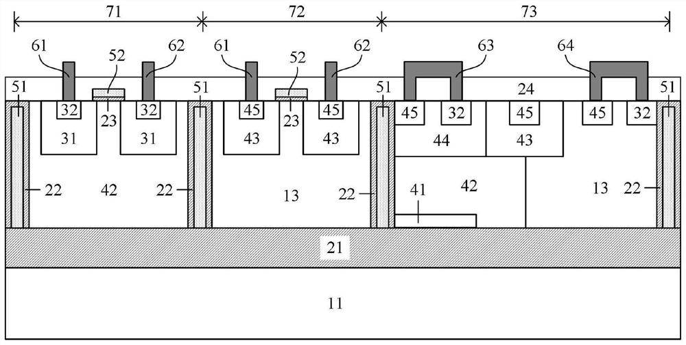
[0040] The invention provides an integrated anti-radiation high-voltage SOI device, the structure of which is as follows figure 1 As shown, it includes a P-type substrate 11, a buried oxide layer 21, and an N-type epitaxial layer 13 formed in sequence; the surface of the N-type epitaxial layer 13 is provided with a high-voltage NMOS device 71, a high-voltage PMOS device 72, and a high-voltage ESD device 73; The integrated radiation-resistant high-voltage SOI device also includes an isolation oxide layer 22, a gate oxide layer 23, a pre-metal dielectric layer 24, a first P-type doped region 41, a second P-type doped region 42, and a third P-type doped region. 43. Fourth P-type doped region 44, fifth P-type doped region 45, first N-type doped region 31, second N-type doped region 32, polysilicon 51, polysilicon gate electrode 52, source metal Electrode 61, drain metal electrode 62, anode metal electrode 63, cathode metal electrode 64; the first N-type doped region 31 is set in t...
Embodiment 2
[0042] The invention also provides a method for manufacturing an integrated radiation-resistant high-voltage SOI device, which is processed and prepared on a silicon-on-insulator material, such as figure 2 As shown, the silicon-on-insulator has a P-type substrate 11, a buried oxide layer 21 and a top layer of silicon 12 stacked sequentially from bottom to top, including the following steps:
[0043] Such as image 3 As shown, the ion implantation process is used to implant P-type impurities on the top layer silicon 12 to form the first P-type doped region 41; the implantation dose of the first P-type doped region 41 is 1E13~1E15cm -2 ;
[0044] Such as Figure 4 As shown, an N-type epitaxial layer 13 is formed on the buried oxide layer 21 by using an epitaxial process; the N-type epitaxial layer 13 covers the first P-type doped region 41;
[0045] Such as Figure 5 As shown, a deep silicon trench is etched on the N-type epitaxial layer 13 by photolithography and etching p...
PUM
 Abstract
Description
Claims
Application Information


