
Image sensor

An image sensor and pixel technology, applied in image communication, TV, color TV components, etc., can solve the problems of large CTIA noise, affecting imaging effect, reducing the signal-to-noise ratio of CMOS image sensors, etc., to reduce output noise, Effect of large full well capacity

Pending Publication Date: 2021-06-29
GPIXEL +1
View PDF9 Cites 0 Cited by
  • Summary
  • Abstract
  • Description
  • Claims
  • Application Information

AI Technical Summary

Problems solved by technology

[0005] Because the CTIA is located on one side of the pixel array, the column bus is too long, the parasitic capacitance at the input end of the CTIA is too large, and the noise of the CTIA is too large, which will reduce the signal-to-noise ratio of the CMOS image sensor and affect the imaging effect.

Method used


Image

  • Image sensor
  • Image sensor
  • Image sensor

Examples


Embodiment Construction

[0021] In order to make the object, technical solution and advantages of the present invention clearer, the present invention will be further described in detail below in conjunction with the accompanying drawings and specific embodiments. It should be understood that the specific embodiments described here are only used to explain the present invention, but not to limit the present invention.

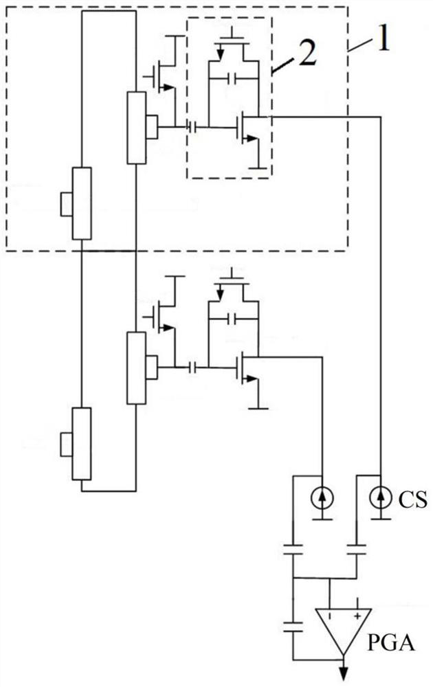
[0022] For traditional image sensors, a column of pixel units share one CTIA, resulting in too long a column bus, excessive parasitic capacitance at the input end of the CTIA, and excessive noise of the CTIA, which will reduce the signal-to-noise ratio of the CMOS image sensor and affect the imaging effect. In order to avoid the problem that the column bus is too long, the present invention adopts the method of controlling and driving the pixels in segments, and divides a pixel into several segments for driving. Each segment is equivalent to a sub-pixel unit, and each sub-pixel unit is ...


PUM


Abstract

The invention provides an image sensor, and the image sensor comprises at least two identical sub-pixel units; each sub-pixel unit comprises a charge exposure transfer structure and a capacitance feedback transconductance amplifier, and each capacitance feedback transconductance amplifier comprises an integrating capacitor, an initialization transistor and a source follower. Two ends of the blocking capacitor are respectively coupled with the charge exposure transfer structure and a grid electrode of the source follower, and a source electrode of the source follower is connected with a reference voltage; two ends of the integrating capacitor are respectively coupled with a grid electrode and a drain electrode of the source electrode follower and are used for carrying out integral amplification on a signal to be output by the source electrode follower, and a source electrode and a drain electrode of the initialization transistor are respectively coupled with two ends of the integrating capacitor and are used for resetting the integrating capacitor. According to the invention, the pixel is divided into a plurality of sub-pixel units for segmented driving, and the CTIA is configured in each sub-pixel unit, so that the parasitic capacitance of the input end of the CTIA is reduced, the noise of the CTIA is reduced, the signal-to-noise ratio of the image sensor is improved, and the imaging effect is improved.

Description

technical field [0001] The invention relates to the technical field of CMOS image sensors, in particular to a CMOS image sensor based on a CTIA pixel structure. Background technique [0002] At present, spectral imaging is widely used in mineral resource exploration, biomedical identification, food detection, atmospheric research and other fields. The spectrometer mainly includes a light source system, a spectroscopic imaging system and a receiving device. The atoms of the elements emit spectral lines under the action of the excitation light source. The spectral lines are separated by the spectroscopic imaging system to form a spectrum. Each element has its own characteristic spectral lines. The intensity of the spectral lines represents the content of the elements in the sample. Each spectrum of the image sensor is photoelectrically converted by the photosensitive array of the image sensor, then analog-to-digital converted by the readout circuit, and finally the data is pr...

Claims


Application Information

Patent Timeline
IPC IPC(8): H04N5/355H04N5/357H04N5/374H04N5/3745H04N5/378
CPCH04N25/59H04N25/616H04N25/772H04N25/76H04N25/75
Inventor 李扬马成刘洋刘芳园
Owner GPIXEL
Features
  • Generate Ideas
  • Intellectual Property
  • Life Sciences
  • Materials
  • Tech Scout
  • Unparalleled Data Quality
  • Higher Quality Content
  • 60% Fewer Hallucinations
Learn More